Digital Circuit
Index 2
74 Series digital circuit of 74141 BCD decimal decoder / driver
Published:2011/7/25 3:14:00 Author:Lucas | Keyword: 74 Series , digital circuit , BCD decimal decoder, BCD decimal driver

It can drive inflated cold-cathode display tube directly; all decoding input could ensure that all outputs of invalid code are off; the maximum reverse current of NPN output transistor is 50mA whenunder 55V.
(View)
View full Circuit Diagram | Comments | Reading(1814)
74 Series digital circuit of 74LS320 crystal-controlled oscillator
Published:2011/8/1 20:51:00 Author:Lucas | Keyword: 74 Series , digital circuit, crystal-controlled oscillator


The working frequency range of crystal-controlled oscillator/ clock pulse is 1Hz ~ 20MHz; TTL level and high level(5V-12V) have 2-phase output.
(View)
View full Circuit Diagram | Comments | Reading(990)
74 Series digital circuit of 74283,74LS283 4-bit binary full adder (with carry lookahead)
Published:2011/8/1 20:52:00 Author:Lucas | Keyword: 74 Series , digital circuit , 4-bit binary , full adder , carry lookahead


The functions are similar to 7483A, 74LS83A, and the table is same with the 7483A.
(View)
View full Circuit Diagram | Comments | Reading(14631)
74 Series digital circuit of 74S281 4-bit parallel binary accumulator
Published:2011/8/1 20:52:00 Author:Lucas | Keyword: 74 Series, digital circuit , 4-bit parallel , binary accumulator


There are 15 arithmetic, logical operations; it has a full shift function; it can be extended full-ahead position N-bit words.
fo, f1, f2,f3 = the corresponding steady input level of F1, F2, F3, F4. QA0, QB0, QC0, QD0= the corresponding level of QA, QB, QC, QD before the establishment of steady-state input conditions. QAn, QBn, QCn= the corresponding level of QA, QB, QC at the latest time hopping.
(View)
View full Circuit Diagram | Comments | Reading(1582)
74 Series digital circuit of 74LS258,74F258 four 2-to-1 data selector (tristate, inverted)
Published:2011/8/9 3:29:00 Author:Lucas | Keyword: 74 Series , digital circuit , four 2-to-1 , data selector , tristate , inverted


Tristate output is connected to the system bus interface directly, and 74LS258A absorption current is twice large than the 74LS258.
(View)
View full Circuit Diagram | Comments | Reading(1121)
74 Series digital circuit of 74LS242/243 four-bus transceiver (tristate) / line driver
Published:2011/8/9 3:30:00 Author:Lucas | Keyword: 74 Series, digital circuit , four-bus transceiver , tristate , line driver


It can make dual-channel asynchronous communication between the data bus; the state of the control input determines the direction of data flowing and the data port model; 242 is the tri-state inverting output, and 243 is the three-state in-phase output. If the transceiver is allowed in both directions at the same time, it may occur destructive oscillation.
(View)
View full Circuit Diagram | Comments | Reading(1218)
74 Series digital circuit of 74LS240,74F240 eight inverting buffer/line driver/ line receiver(three-state)
Published:2011/8/1 20:52:00 Author:Lucas | Keyword: 74 Series , digital circuit , eight inverting buffer, line driver, line receiver, three-state


When 1G and 2G are H at the same time, Y=high resistance;when 1G and 2G are L at the same time, Y=A.
(View)
View full Circuit Diagram | Comments | Reading(1044)
74 Series digital circuit of 74199 8-bit shift register
Published:2011/8/1 20:52:00 Author:Lucas | Keyword: 74 Series , digital circuit, 8-bit shift register


Parallel storage; right shift(direction is from the QA to QH): left shift(direction is from the QH to QA); it forbids the clock.a. .. h= the input of steady-state input level of A to H.QAo, QBo, QGo, QHo=the corresponding level level of QA, QB, QG, QH before building the specified steady state.QAn, QBn..QGn= the corresponding level of QA, QB to QGbefore the next jump of the clock.
(View)
View full Circuit Diagram | Comments | Reading(1211)
74 Series digital circuit of 74196/74197 preset decimal/binary counter
Published:2011/8/1 20:53:00 Author:Lucas | Keyword: 74 Series, digital circuit , preset decimal counter, binary counter


196 can make BCD binary/quinary count, and 197 is the binary counter.
(View)
View full Circuit Diagram | Comments | Reading(1735)
74 Series digital circuit of 74LS395A,74F395 4-bit cascadable shift register (tristate)
Published:2011/8/1 22:50:00 Author:Lucas | Keyword: 74 Series , digital circuit , 4-bit cascadable, shift register , tristate

It is the tri-state 4-bit cascaded parallel input and output shift register; 74LS395A absorption current is three times greater than 74LS395. When output control is high, the tri-state output disable is high impedance, but the timing work and QD output of the register is not affected.
a~ d = the corresponding steady input level of A~ D. QA0~ QD0= the corresponding level of QA~QD before the establishment of steady-state input conditions. QAn~ QDn= the corresponding level of QA~ QD at the latest time hopping.
(View)
View full Circuit Diagram | Comments | Reading(1106)
74 Series digital circuit of 74LS384, 74F384 8-bit × 1-bit complement multiplier
Published:2011/8/2 1:00:00 Author:Lucas | Keyword: 74 Series , digital circuit , 8-bit × 1-bit , complement multiplier


2's complement multiplication; it is only multiplied by the absolute value; it can be cascaded to any bit; 8-bit multiplied data parallel input; multiplier data serial input; product data serial output; LS384 typical maximum clock frequency is 40MHz; when is is cascaded,the output of a circuit is connected to K input of the next circuit, and the circuit contains the highest level can be indicated by the model input.
(View)
View full Circuit Diagram | Comments | Reading(1573)
74 Series digital circuit of 74LS373, 74ALS373 octal D-latch(tristate)
Published:2011/8/1 23:01:00 Author:Lucas | Keyword: 74 Series , digital circuit , octal D-latch, tristate

Tristate output; the load full parallel access; buffer control input; 74LS363 is similar to 74LS373, but has the high VOH with MOS interface.
Q0 = the output level before establishing the steady-state input conditions.
(View)
View full Circuit Diagram | Comments | Reading(5056)
74 Series digital circuit of 74LS362 four-phase clock generator / driver
Published:2011/8/1 22:56:00 Author:Lucas | Keyword: 74 Series , digital circuit , four-phase clock generator , four-phase driver
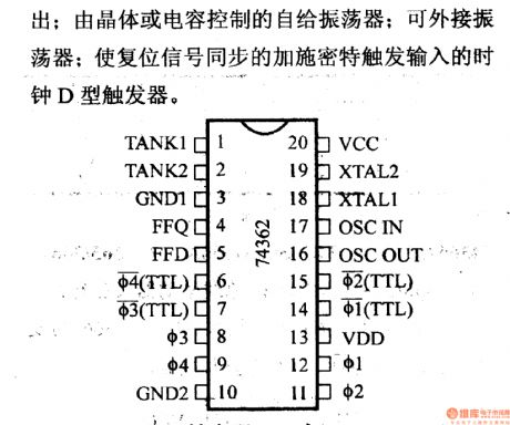
It is used as TMS9900 or other microprocessor clock generator/ driver; high four-phase output; complementary TTL four-phase output; it is the self-support oscillator controlled by the capacitor and crystal; it can connect external oscillator; the reset signal is synchronized by the clock D flip-flop with the Schmitt trigger input.
(View)
View full Circuit Diagram | Comments | Reading(1734)
74 Series digital circuit of 74LS354/356 8-to-1 data selector(tristate with address latching)
Published:2011/8/2 0:43:00 Author:Lucas | Keyword: 74 Series, digital circuit , 8-to-1 data selector, tristate , address latching
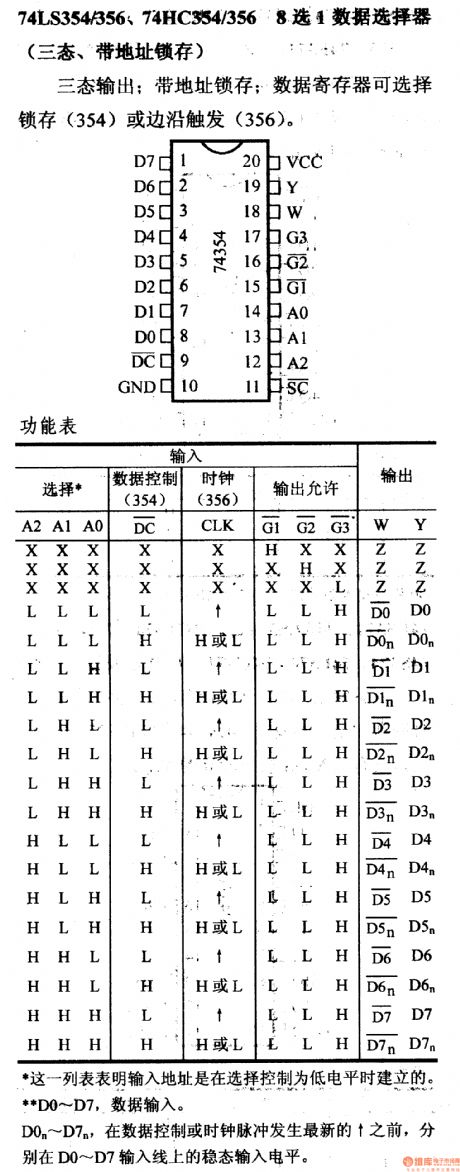
This list shows that the input address is established when the control is low. D1 ~ D7 are the data input. D0n ~ D7n are the steady state input level in D0 ~ D7 line before the latest increasing of the data control or clock pulse.
Three-state output with address latching; data register can choose data latch(354) or edge-triggered (356).
(View)
View full Circuit Diagram | Comments | Reading(752)
74 Series digital circuit of 74LS352, 74F352 dual 4-to-1 data selector(inverting)
Published:2011/8/1 20:49:00 Author:Lucas | Keyword: 74 Series , digital circuit , dual 4-to-1 , data selector, inverting

The selecting inputs A and B are used in common.
(View)
View full Circuit Diagram | Comments | Reading(803)
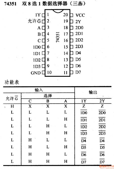
74 Series digital circuit of 74351 dual 8-to-1 data selector(tristate)
Published:2011/8/1 20:43:00 Author:Lucas | Keyword: 74 Series, digital circuit , dual 8-to-1 , data selector, tristate
View full Circuit Diagram | Comments | Reading(677)
74 Series digital circuit of 74LS299, 74S299 8-bit bidirectional universal shift/storage registers
Published:2011/8/2 4:36:00 Author:Lucas | Keyword: 74 Series , digital circuit , 8-bit bidirectional, universal shift, storage registers
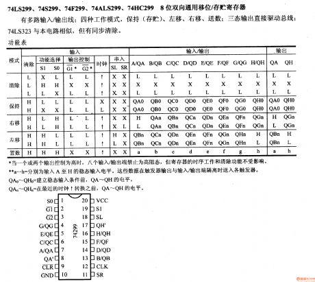
It has multi-road / output lines and four modes to maintain (store) left, right shift and output number; three-state outputs can directly drive the bus; 74LS323 is similar to the circuit, but it has the synchronous clear function. When one or two output controlling is high, eight input / output ends against in high-impedance state, but the timing register and cleaning functions are not affected. The data is input to each trigger when the flip-flop output and input ends are isolated.
QA10~QH0 is the level of QA~QH before the establishment of steady-state input conditions. QAn~QHn=the level of QA~QH before the latest time hopping.
(View)
View full Circuit Diagram | Comments | Reading(1583)
74 Series digital circuit of 74LS323,74S323 8-bit bidirectional universal shift/storage registers
Published:2011/8/2 4:34:00 Author:Lucas | Keyword: 74 Series, digital circuit , 8-bit bidirectional , universal shift, storage registers

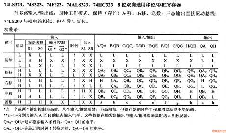
It has multi-road / output lines and four modes to maintain (store) left, right shift and output number; three-state outputs can directly drive the bus; 74LS299 is similar to the circuit, but it has the asynchronous reset. When one or two output controlling is high, eight input / output ends against in high-impedance state, but the timing register and cleaning functions are not affected. The data is input to each trigger when the flip-flop output and input ends are isolated.
QA10~QH0 is the level of QA~QH before the establishment of steady-state input conditions. QAn~QHn=the level of QA~QHbefore the latest timehopping.
(View)
View full Circuit Diagram | Comments | Reading(860)
74 Series digital circuit of 74LS322,74F322 sign-extended 8-bit shift register
Published:2011/8/2 3:55:00 Author:Lucas | Keyword: 74 Series, digital circuit , sign-extended 8-bit , shift register
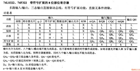
Multiple input / output; tri-state outputs can directly drive the bus; it has signed extended function; it can be direct unconditional cleared. When the output allows for high, eight input / output ends can not be in a high-impedance state, but does not affect the timing operation or clear of registers, for example, if the register allows the input and S / P input, the clear input are low, the register is removed, and eight input / output ends can not be in a high-impedance state.
QA0 ...QH0= QA ...QH level before the establishment of steady-state input conditions.
D0, D1=the steady input level ofinput ends D0, D1
a..h =the steady input level of the input ends of A to H.
(View)
View full Circuit Diagram | Comments | Reading(751)
74 Series digital circuit of 74LS295B 4-bit bidirectional universal shift register (tristate)
Published:2011/8/2 4:24:00 Author:Lucas | Keyword: 74 Series , digital circuit , 4-bit bidirectional , universal shift register , tristate


Absorption current is three times greater than LS295A; parallel input, parallel output; it has three operation modes with parallel register, and the right shift(direction is from QA to QD), left shift(the direction is from QD to QA). Data is input at the D-side.
a, b, c, d = the corresponding steady input level of A, B, C, D.
QA0, QB0, QC0, QD0= the corresponding level of QA, QB, QC, QD before the establishment of steady-state input conditions.
QAn, QBn, QCn= the corresponding level of QA, QB, QC at the latest time hopping.
(View)
View full Circuit Diagram | Comments | Reading(1159)
| Pages:2/19 12345678910111213141516171819 |
Circuit Categories
power supply circuit
Amplifier Circuit
Basic Circuit
LED and Light Circuit
Sensor Circuit
Signal Processing
Electrical Equipment Circuit
Control Circuit
Remote Control Circuit
A/D-D/A Converter Circuit
Audio Circuit
Measuring and Test Circuit
Communication Circuit
Computer-Related Circuit
555 Circuit
Automotive Circuit
Repairing Circuit
