
Index 244
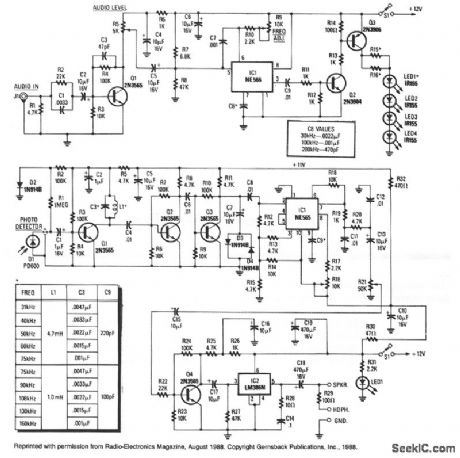
PERSONAL_POCKET_PAGER
Published:2009/7/7 9:21:00 Author:May
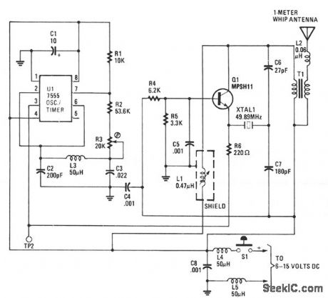
When activated, the transmitter sends out a 49.890-MHz, AM rf carrier. The receiver detects, ampli-fies, and decodes the rf signal, which, in turn, activates a piezo buzzer. The receiver is small enough to carry in a pocket or sit on your workbench, The transmitter is also small and fits easily into a pocket for quick access. (View)
View full Circuit Diagram | Comments | Reading(688)
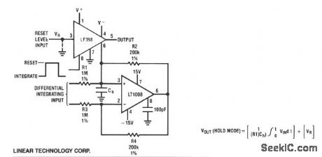
INTEGRATOR_WITH_PROGRAMMABLE_RESET_LEVEL
Published:2009/7/7 9:16:00 Author:May
View full Circuit Diagram | Comments | Reading(477)
RESETTABLE_INTEGRATOR
Published:2009/7/7 9:14:00 Author:May

The low rDS(on) and high peak current capability of the DG419 makes it ideal for discharging an integrator capacitor. A high logic input pulse disconnects the integrator from the analog input and discharges the capacitor. When the logic input lowers, the integrator is triggered. D1 and D2 prevent the capacitor from charging to over 15 V. (View)
View full Circuit Diagram | Comments | Reading(1320)
565_SCA_DEMODULATOR
Published:2009/7/7 8:48:00 Author:May
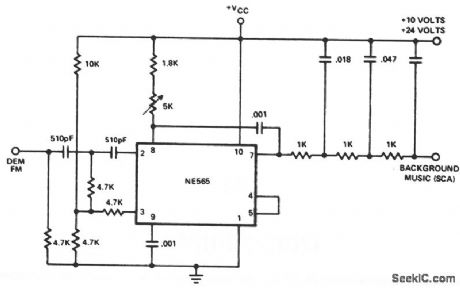
This application involves demodulation of a frequency-modulated subcarrier of the main channel. This popular example uses the PLL to recover the SCA (Subsidiary Carrier Authorization or storecast music) signal from the combined signal of many commercial FM broadcast stations. The SCA signal is a 67 kHz frequency-modulated subcarrier which puts it above the frequency spectrum of the normal stereo or monaural FM program material. By connecting the circuit to a point between the FM discriminator and the deemphasis filter of an FM receiver and tuning the receiver to a station which broadcasts an SCA signal, you can obtain hours of commercial-free background music. (View)
View full Circuit Diagram | Comments | Reading(1268)
ADJUSTABLE_DELAY
Published:2009/7/7 8:47:00 Author:May

You can obtain well over 360 ° of phase delay by cascading two monostable multivibrators. In a typical configuration, a single monostable multivibrator is used to introduce delay in a pulse train; the multivibrator triggers on each incoming pulse, provided it resets in time for the next pulse. Yet even when it resets in time, the single monostable multivibrator provides a maximum phase delay of less than 360 °. However, with the cascaded-multivibrator approach, you can achieve 650 ° of phase delay by using an input-pulse spacing of 200 μs for example, with the component values shown. Every input pulse will trigger the circuit while you adjust the phase delay throughout its available range. The first multivibrator triggers the second one, whose reset marks the total delay time (2t). Each introduces a delay of t μs, based on 0.01-μF timing capacitors and equal charging currents from the three-transistor, dual-current source. The two multivibrator arrangement allows the first multivibrator to reset in time to be triggered by the next input pulse. Also, the variation of t is linear with the potentiometer setting. (View)
View full Circuit Diagram | Comments | Reading(1173)
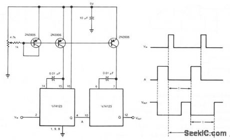
PULSE_DELAY_WITH_DUAL_EDGE_TRIGGER
Published:2009/7/7 8:44:00 Author:May

A single monostable multivibrator delays a pulse train by a variable amount; nonetheless, this amount can be no less than the minimum allowed pulse width tw The exclusive-OR gate, IC1, generates a short pulse following every leading or falling edge of the input waveform. These pulses cause one-shot IC2 to produce a negative-going pulse with a duration equal to the desired time delay tp which you set by adjusting potentiometer R. Flip-flop IC3 then creates a delayed replica of the input pulse by latching the Q1 out-put of IC2 between positive-going transitions. You can independently control the output-pulse duration by cascading a second one shot with the first. (View)
View full Circuit Diagram | Comments | Reading(732)
LEADING_EDGE_DELAY
Published:2009/7/7 8:42:00 Author:May

Circuit (a) lets you delay the leading edge of a positive pulse while leaving the trailing edge almost unaffected. A positive input transition, inverted by IC2, has no effect on IC1B. However, when the positive transition reaches IC1A, (delayed by the adjustable network of R1, R2, and C1), it toggles both NOR gates, initiating the output pulse. When the input decreases IC1B follows suit, delayed only by the propagation through itself and IC2. Circuit (b) produces an inverted output pulse. Inverter IC1 serves as a buffer for the signal source-an advantage when driving a low-impedance (short-delay) network. Moreover, only the propagation delay of IC2B separates the output's trailing edge from that of the input. You can configure circuit (a) to handle negative pulses by using NAND instead of NOR gates. Similarly, circuit (b) will produce a delayed positive pulse in response to negative input pulse, if you substitute NOR gates for NAND gates.
(View)
View full Circuit Diagram | Comments | Reading(673)
IR_RECEIVER
Published:2009/7/7 8:21:00 Author:May

Infrared emissions detected by Q1 are fed through U1a to U1b, which amplifies the signal by a factor of 100. The amplified output of U1b is fed to U1c through R9, C2, and R6. Potentiometer R9 serves as a volume control. With R9 set to pass the maximum signal, U1c provides a gain of 100, for a total system gain of 10,000 dB. The output of U1c is connected to voltage follower circuit U1d to better match and drive headphones that can be plugged into J1. (View)
View full Circuit Diagram | Comments | Reading(1496)
INFRARED_WIRELESS_SPEAKER_SYSTEM
Published:2009/7/7 8:17:00 Author:May

Although the IR region is free from radio interference, it is subject to interference front incandescent lamps, fluorescent lamps, stray reflections, and other sources.A simple way to overcome that problem is to create a carrier by chopping the IR radiation at a rate of 100 kHz. The audio then modulates the carrier by modulating the chopping rate. A receiver then detects the IR beam as a 100-kHz FM signal. The only disadvantage is that instead of a simple audio amplifier, a high-gain FM receiver is necessary. However, with the ICs that are now available, an FM receiver is easy to build, and contains little more circuitry than a high-gain audio amplifier. The kit is available from North Country Radio, P.O. Box 53, Wykagyl Station, NY 10804. (View)
View full Circuit Diagram | Comments | Reading(1530)
FURNACE_EXHAUST_GAS_TEMPERATURE_MONITOR_WTH_LOW_SUPPLY_DETECTION
Published:2009/7/7 7:13:00 Author:May

This circuit can be used to measure exhaust gas temperature m a furnace. The 10-bit LTC1091A gives 0.5°C resolution over a 0°C to 500°C range. The LTC1050 amplifies and filters the thermocouplesignal, the LT1025A provides cold junction compensation and the LT1019A provides an accurate reference. The J-type thermocouple characteristicis linearized digitally inside the MCU. Linear interpolationbetween known temperature points spaced 30°C apart introduces less than 0.1°C error.The 20-K/10 ΚΩdivider on CH1 of the LTC1091 provides low supply voltage detection,Remote locationis easy, with datatransferred from the MCU to the LTC1091 via the three wlre serial part. (View)
View full Circuit Diagram | Comments | Reading(720)
CRYSTAL_TIMEBASE
Published:2009/7/7 7:12:00 Author:May

An on-board oscillator and a 17-stage divider compose IC1. By connecting a standard 3.58-MHz, television color-burst crystal as shown, an accurate source of 60-Hz squarewaves is generated at the IC's output, pin 1. Those pulses are then fed to IC2, a 4024 seven-stage ripple counter. Its outputs are connected to different gates in IC3, which is a dual four-input NAND gate. Depending on which position pulse-select switch S2 is on, one of those gates will provide an output/reset pulse of the selected width. (View)
View full Circuit Diagram | Comments | Reading(1187)
ELECTRONIC_DICE
Published:2009/7/7 7:00:00 Author:May

The basic die circuit is given. A 555 timer, IC1, is connected as an astable multivibrator. This feeds clock pulses to divide-by-six counter IC2 the outputs of which are decoded by gates N1 to N6 to drive an array of LEDs in the familiar die pattern. When switch S1 is in position b, the reset input of IC1 decreases and the oscillator is inhibited. Power is fed to the LEDs via Slb so that the display is activated. When the die is rolled 'oy switching 51 to position a, the display is blanked. C4 is connected to positive supply via Sla, producing a short pulse which resets IC2 via N7 and N8. The reset input of IC1 is pulled high via R5, so the multivibrator begins to oscillate and feeds clock pulses to IC2 via NS. When S1 is switched back to position a, the multivibrator is again inhibited. Then, the counter stops and power is applied to the LEDs which display the value of the throw. (View)
View full Circuit Diagram | Comments | Reading(0)
COIN_FLIPPER
Published:2009/7/7 6:56:00 Author:May

The circuit is basically a 555 astable circuit that divides two LEDs, LED1 and LED2. LED2 is switched on when the output of U1 is high, and LED1 is activated when its output is low. When U1 oscillates, LED1 and LED2 switch on alternately as the output of U1 switches from state to state. Resistor R1's value is high in comparison to R2, so the waveform at the output is a square wave with a mark/space ratio of nearly one-to-one. When you release S1, you break the circuit and U1 latches whatever the output state happens to be at the time. (View)
View full Circuit Diagram | Comments | Reading(1318)
ASTABLE_MULTIVIBRATOR
Published:2009/7/7 6:39:00 Author:May

The power bandwidth of the HA-5147 extends the circuit's frequency range to approximately 500 kHz. Rt can be made adjustable to vary the frequency if desired. Any timing errors because of VOSorIbias have been minimized by the precision char-acteristics of the HA-5147. D1 and D2, if used, should be matched to prevent additional timing errors. These clamping diodes can be omitted by tying Rt and positive feedback resistor Rf directly to the output. (View)
View full Circuit Diagram | Comments | Reading(0)
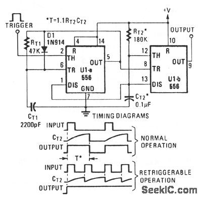
RETRIGGERABLE_ONE_SHOT
Published:2009/7/7 6:36:00 Author:May
View full Circuit Diagram | Comments | Reading(488)
LOW_FREQUENCY_MULTIVIBRATOR
Published:2009/7/7 6:35:00 Author:May
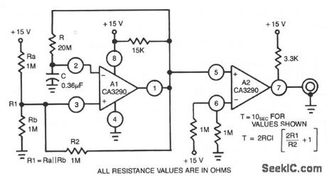
This circuit uses half the CA3290 BiMOS dual voltage comparator as conventional multivibrator. The second half maintains frequency against effects of output loading. Large values of timing resistor, R1, assure long time delays with low-leakage capacitors. (View)
View full Circuit Diagram | Comments | Reading(485)
LINEAR_RAMP_MONOSTABLE
Published:2009/7/7 6:34:00 Author:May
View full Circuit Diagram | Comments | Reading(437)
PROGRAMMABLE_FREQUENCY_ASTABLE
Published:2009/7/7 6:33:00 Author:May
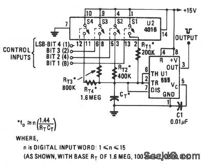
View full Circuit Diagram | Comments | Reading(1531)
PROGRAMMABLE_FREQUENCY_FREE_RUNNING_MULTIVIBRATOR
Published:2009/7/7 6:29:00 Author:May
This is the simplest of any programmable oscillator circuit, since only one stable timing capacitor is required. The output square wave is about 25 V pk-pk, and has rise and fall times of about 0.5 μs. If a programmable attenuator circuit is placed between the output and the divider network, 16 frequencies can be produced with two HA-200's and still only one timing capacitor. (View)
View full Circuit Diagram | Comments | Reading(620)
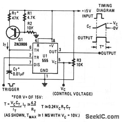
MONOSTABLE_OPERATION
Published:2009/7/7 6:28:00 Author:May
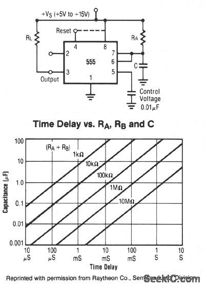
In this mode, the timer functions as a one shot. The external capacitor is initially held discharged by a transistor internal to the timer. Applying a negative trigger pulse to pin 2 sets the flip-flop, driving the output high, and releasing the short circuit across the external capacitor. The voltage across the capacitor increases with the time constant r = RAC to 2/3 VS, where the comparator resets the flip-flop and discharges the external capacitor. The output is now in the low state.Circuit triggering takes place when the negative-going trigger pulse reaches 1/3 VS; the circuit stays in the output high state until the set time elapses. The time the output remains in the high state is 1.1 RAC and can be determined by the graph. A negative pulse applied to pin 4 (reset) during the timing cycle will discharge the external capacitor and start the cycle over again beginning on the positive-going edge of the reset pulse. If reset function is not used, pin 4 should be connected to Vs to avoid false resetting. (View)
View full Circuit Diagram | Comments | Reading(497)
| Pages:244/471 At 20241242243244245246247248249250251252253254255256257258259260Under 20 |
Circuit Categories
power supply circuit
Amplifier Circuit
Basic Circuit
LED and Light Circuit
Sensor Circuit
Signal Processing
Electrical Equipment Circuit
Control Circuit
Remote Control Circuit
A/D-D/A Converter Circuit
Audio Circuit
Measuring and Test Circuit
Communication Circuit
Computer-Related Circuit
555 Circuit
Automotive Circuit
Repairing Circuit