
A/D-D/A Converter Circuit
Index 4
UP_DOWN
Published:2009/7/16 3:47:00 Author:Jessie

Circuit shown was developed for use in 5645.8-kHz IF amplifier of Drake R-4B amateur-band receiver, to utilize high-performance characteristics of Sherwood Engineering CF-125/8 CW crystal filter having bandwidth of only 125 Hz. Texas Instruments TL442 double-balanced mixers convert IF signal to 5695-kHz center frequency of filter and convert filter output back to IF value. Same crystal oscillator serves for both upconversion and downconversion. Gives true single-signal reception. Article covets procedures for interfacing any crystal filter with any receiver IF value. -H. Sartori, An Up/Down Filter Converter, Ham Radio, Dee. 1977, p 20-25. (View)
View full Circuit Diagram | Comments | Reading(1944)
8_30_MHz_AMATEUR_BANDS
Published:2009/7/16 3:41:00 Author:Jessie

Will convert any frequency in tuning range to IF value between 3.5 and 4 MHz. Requires only three transistors and one IC. D1 and D2 can be germanium or silicon, such as 1N914 D3 is rectifier diode. Q2 can be almost any general-purpose high-frequency transistor. Two of gates in SN7400N TTL IC serve as crystal oscillator, and other two gates are buffers for detector diodes D1 and D2. Diodes are modulated by VCO Q2. Detector out, put is amplified and filtered by Q1 to produce control voltage for tuning D3. Output from mixer Q3 is untuned, with RFC as drain load element. -R. Megirian, High Frequency Utility Converter, 73 Magazine, June 1977, p 50-53. (View)
View full Circuit Diagram | Comments | Reading(1646)
432_MHz_TO_28_MHz
Published:2009/7/16 3:39:00 Author:Jessie

Contains bandpass filter, grounded-grid RF amplifier stages Q15-Q16,mixer Q17、and crystal oscillator Q18-Q19,Developed for use in all-band double-conversion superheterodyne receiver for AM narrow-band FM, CW, and SSB operation. Supply is 13.6 V regulated Article gives all circuits of receiver,-D. M. Eisenberg, Build This All-Band VHF Receiver 73Magazine, Jan 1975、p 105-112 (View)
View full Circuit Diagram | Comments | Reading(4107)
28_30_MHz_TO_165_MHz
Published:2009/7/16 3:37:00 Author:Jessie

10-meter tuner gives excellent image suppression with 1.65-MHz output, for feeding into inexpensive receiver having 1.65.MHz IF. Tuning capacitors are three-gang Miller 1460-1. Article gives all coil data along with construction details.-B. Hoisington, Tuneable 10 Meter Converter, 73 Magazine, Jan, 1974, p 57-62. (View)
View full Circuit Diagram | Comments | Reading(1291)
BELOW_BROADCAST_BAND
Published:2009/7/16 3:35:00 Author:Jessie

Simple solidstate converter can be used with any good communication receiver covering 3.5-4 MHz to bring in stations from 5-550 kHz (200 meters and up). Input coil L1 is changed from 0.28 H for 5-11 kHz to 120 μH for 250-550 kHz in eight steps, as given in article. C2 consists of two 3-gang variable capacitors with stators wired in parallel, gang-tuned with dial cords. Trimmer C7 is 1-12 pF, adjusted to give reliable starting of FT-2433500-kHz crystal. L2 is 80-90 μH for 80 meters, and loopstick is for broadcast band. -K. Cornell, 200 Meters and Up Receiving Converter for Low Frequencies, Ham Radio, Nov. 1976, p 24-26. (View)
View full Circuit Diagram | Comments | Reading(1288)
1296_MHz_TO_285_MHz
Published:2009/7/16 3:34:00 Author:Jessie

Uses UHF transistors in active mixer and in final stage of injection chain, for lower noise figure and useful conversion gain. Doubler and tripler stages are individually shielded. -L. Crutcher, An Active-Mixer Converter for 1296 MHz, QST, Aug. 1974, p 11-14. (View)
View full Circuit Diagram | Comments | Reading(1976)
WWV_FET_CONVERTER
Published:2009/7/16 3:30:00 Author:Jessie

Receives WWV on 2.5, 5, 10, 15, ver operating and 20 MHz using modified transistor AM broadcast receiver operating straight-through for for 2.5.MJz reception and serving as IF amplifier for converter when tuned to higher WWV and WWVH frequencies. Only two crystals are needed because each allows reception of two WWV frequencies; thus, 10 and 20 MHz, are image frequencies when receiving 5 and 15 MHz. Loopstick antenna, of radio is replaced with small slug-tuned coil L6 to use 2.5-MHz image frequency when radio is tuned to 1590 kHz. Converter uses –dual-gate MOS FETs in RF stang Q1 and mixer Q2, with JFET Q3 as oscillator Antenna is short piece of wire. -H. Olson, Five-Frequency Receiver for WWV, Ham Radio, July 1976, P 36-38. (View)
View full Circuit Diagram | Comments | Reading(3109)
20_METERS_TO_40_METERS
Published:2009/7/16 3:28:00 Author:Jessie

Used with 40-meter receiver for which circuit is also given. Converter output is in 40-meter band, for direct feed to input of receiver. L4 is 12 turns No. 26 enamel on Amidon FT37-61 toroid, L5 is 24 turns No. 26 enamel on Amidon 7-50-6 toroid, and T3 uses Amidon 7-50-6 toroid with 2 turns No. 26 enamel for primary and 21 turns for secondary. -D. DeMaw, The Mini-Miser's Dream Receiver, QST, Sept. 1976, p 20-23. (View)
View full Circuit Diagram | Comments | Reading(2231)
VFO_CONVERTER
Published:2009/7/16 3:25:00 Author:Jessie

Used in solid-state five-band communication receiver. VFO input (5-5.5 MHz) goes directly to amplifiers Q5 and Q6 when bandswitch is on 3.5 or 14 MHz. When VFO signal is applied to balanced mixer CR7-CR10, product is at 9 MHz. Diodes should be carefully selected for equal voltage drops t20 mV at various current values such as 0.75, 2, 10, and 20 mA. When bandswitch is on 7, 21, or 28 MHz, VFO signal is mixed with output of FET crystal oscillator and filtered before being applied to Q5 and Q6. FET oscillators a1-a4 are energized by +12 V from bandswitch, with diodes CR1-CR4 selecting output. Crystals are parallel-resonant with 32-pF Load. Y2, Y3, and Y4 are third-overtone type.-P. Moroni, Solid-State Communications Receiver, Ham Radio, Oct. 1975, p 32-41. (View)
View full Circuit Diagram | Comments | Reading(1823)
165_MHz_TO_135_kHz
Published:2009/7/16 4:00:00 Author:Jessie

Provides good selectivity, good AVC, and smooth tuning.Article gives coil-Winding data,-B. Hoisington, Miniboxing the 432er Receiver, 73 Magazine, Jan,1975、p46-52, (View)
View full Circuit Diagram | Comments | Reading(1150)
144_MHz_TO_14_MHz
Published:2009/7/16 3:58:00 Author:Jessie

Oscillator uses 43.333-MHz overtone-cut crystal feeding class A tripler that injects 130-MHz signal into gate of MPF-102 mixer for combining with 144-MHz output of IGFET BF amplifier to give 14 MHz for amateur-band or general-coverage receivers. Article covers construction and alignment, including de-tailed coil-winding data. -C. Klinert, A Two Meter Converter, 73 Magazine, Sept. 1973, p 65-67. (View)
View full Circuit Diagram | Comments | Reading(2796)
TRANSDUCER_VOLTAGE_RESISTANCE_CONVERTER
Published:2009/7/16 5:47:00 Author:Jessie

D-c voltage output of transducer is converted to a-c voltage by fet in one leg of bridge that controls f-m oscillator.Arrangement converts transducer in effect to variable resistor, simplifying measurement of many parameters in data acquisition system.-A. R. Greenfield and W. H. McCloskey, FET Converts Transducer for Use in A-C Bridge Electronics, 39:3, p 84-85. (View)
View full Circuit Diagram | Comments | Reading(1123)
LOW_NOISE_DC_TO_DC_CONVERTER
Published:2009/7/13 3:00:00 Author:May

Low noise is achieved by this inexpensive and versatile 5-V-to-±12-V dc-to-dc converter. Wide-band output noise appears to be well under 500 μV p-p. The converter accepts external clocks from 80 to 120 kHz. The converter operates much like a TV horizontal deflection circuit. Q3 is a logic-level power MOSFET driven by an external clock. When Q3 is switched on, current ramps up through T1's primary. When Q3 is switched off, Q3's drain flies back to 25 Y as C4 resonates with T1's primary, transferring energy to the secondary. As the flyback voltage falls and attempts to go below ground, the intrinsic diode of the power MOSFET clamps it. In addition, the excess resonant energyflows backward through T1's primary, recharging C1. When this point is reached, Q3 is again switched on and the cycle repeats. Q3's gate (trace 2) is switched on and off when Q3's drain is near ground. Q3's gate driver power requirements are modest enough to be handled by any 74HC logic gate. Regulation is achieved by the error amplifier (LT1013). Despite the fact that Q1 acts as a linear pass transistor, converter efficiency can exceed 75 percent if the voltage drop across Q1 is minimized. This can be accornplished by either adjusting the clock frequency or tuning C4 to adjust the flyback voltage. (View)
View full Circuit Diagram | Comments | Reading(2828)
500_kHz_5_V_TO_12_V_400_mA_DC_TO_DC_CONVERTER
Published:2009/7/13 2:14:00 Author:May

In some 5-V-only systems, it is necessary to generate a local 12-V supply to power op amps, data-acquisition circuitry, or devices, such as small motors. The LT1372 is a 500-kHz high-efftciency switching power regulator that provides this capability, as shown in this circuit. The 500-kHz switching frequency reduces the size of the magnetics significantly over that in lower-frequency designs; they consume just 0.5 in2 oftotal board space. The internal switches are current-limited to 1.5 A. In addition, the quiescent current gf LT1372 is just 4 mA, which, along with very low switch losses, provides up to 89 percent efficiency in this application. Other features of the LT1372 include synchronization of the switching action to a system clock source and shutdown capability, reducing supply currents to just 12 μA. Also, the LT1372 has two feedback inputs that allow regulation of either positive or negative output voltages. (View)
View full Circuit Diagram | Comments | Reading(1055)
DUAL_OUTPUT_500_kHz±15_V_DC_TO_DC_CONVERTER
Published:2009/7/13 2:11:00 Author:May

The LT1371 dual-output flyback converter circuit shown generates ±15 V at 200 mA each from a 5-V supply. The LT1371 is a 500-kHz high-efficiency switching regulator with 3-A power switch, yet it uses only 4 rnA typical quiescent current. The high operating frequency allows a small surfacemount, dual-output winding flyback transformer to be used. Each output is monitored by separate positive and negative feedback inputs on the LT1371 to be sure that neither output rises above its set point. This removes a common problem in dual-output designs using a single controller: the tendency of the voltage of the least loaded output to fly high. Output voltage regulation is best when both outputs are evenly loaded. (View)
View full Circuit Diagram | Comments | Reading(2948)
3_TO_7_V_DC_TO_DC_CONVERTER
Published:2009/7/13 2:09:00 Author:May

Converting the voltage from a four-cell battery pack to 5 V while using the full capacity of the batteries requires two modes of operation: step-down from an input voltage of 6 V and step-up from an input of 4 V (or less). A flyback topology can accomplish this, but uses a costly custom transformer. The LT1300 circuit shown utilizes the simple SEPIC topology, and is capable of 220 mA of output current at 5 V from a minimum 3-V input. The two inductors specified are available off the shelf. The circuit uses a boost section and a buck, or step-down, section, with the two inductors (L1 and L2) and two capacitors (C2 and C3) all acting as energy-storage elements. Efficiency is slightly less than that of a direct step up (see graph), but is better than that of an equivalent flyback configuration. Other features of the circuit include shutdown (10 μA max. supply current) with full input-to-output isolation, which allows the output to go to zero volts, yet present no load to the batteries.Also, either a 3.3-V or 5-V output can be selected by using the logic-select pin of the LT1300. (View)
View full Circuit Diagram | Comments | Reading(1040)
9_V_DC_TO_DC_CONVERTER
Published:2009/7/13 2:06:00 Author:May


In portable applications, 9-V batteries are frequently used. For low-power dc-to-dc step-down conversion, the LTC1174 is a simple integrated solution. With its internal MOSFET power switch, the LTC1174-5 requires only four extemal parts to achieve 90-percent efficiency. All surface-mount assembly is standard, with high-frequency operation at up to a 200 kHz switching frequency. Extremely low dropout operation is possible because the LTC1174 operates at 100-percent duty cycle with low input voltages. A single logic-level input selects an output voltage of 3.3 V or 5 V. (View)
View full Circuit Diagram | Comments | Reading(1098)
TWO_CELL_5_V_500_mA_CONVERTER
Published:2009/7/13 1:55:00 Author:May

Hand-held instruments, PCMCIA cards, and portable communications gear often require high current for their operation, although only for short periods at a time. Current of 500 mA at 5 V can be obtained from a two-cell battery using a switching regulator controller IC, an external switch transistor, and some discrete components, but the solution is inefficient, space-intensive, and cumbersome. The LT1302 was designed to provide higher output currents by using an integrated 2-A low-loss switch. An output current of 500 mA at 5 V with 85 percent efficiency is possible from two AA cells. Component size is minimized by using a fixed-frequency 220-kHz PWM architecture. The circuit maintains high efficiencies at low load currents by automatically switching to Burst mode operation at lower switch currents. (View)
View full Circuit Diagram | Comments | Reading(1069)
INDUCTORLESS_-5_V_CONVERTER
Published:2009/7/13 1:51:00 Author:May
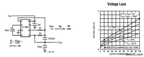
Switched capacitor voltage converters are great for supplying an unregulated negative voltage from a positive supply. To provide a regulated negative voltage, a linear regulator is normally required.The LT1054 eliminates the extra voltage regulator by adding a pair of feedback resistors, as shown here. An internal feedback circuit allows full regulation of the output voltage with changes in input voltage and load cutpent. With a minimum input of 6.5 V, the LT1054 can produce a regulated -5-V output at loads of up to 100 mA max. External components required include four capacitors and two resistors. (View)
View full Circuit Diagram | Comments | Reading(959)
MICROPOWER_POSITIVE_TO_NEGATIVE_CONVERTER
Published:2009/7/13 1:49:00 Author:May

Switched capacitor voltage converters are a convenient way to generate a local negative supply for biasing special circuitry, but have been limited by CMOS processes to 10 V of supply or less. The LTC1144 voltage converter overcomes this limitation, extending the maximum input voltage to 20 V. Still, the part retains the low power of CMOS operation. The LTC1144 circuit shown here generates a negative supply voltage of -13.8 V typ. (-12.6 Vmin) from a 15-V input at a maximum load current of 20 mA. Higher load currents are possible at slightly lower output voltages. The low-cost circuit includes two surface-mount capacitors, minimizing board space. A supply current of 1.2 mA (max.) results in high conversion efficiency, while just 8 μA of supply current is consumed in shutdown, making the LTC1144 excellent for use in battery-powered systems. (View)
View full Circuit Diagram | Comments | Reading(1221)
| Pages:4/24 1234567891011121314151617181920Under 20 |
Circuit Categories
power supply circuit
Amplifier Circuit
Basic Circuit
LED and Light Circuit
Sensor Circuit
Signal Processing
Electrical Equipment Circuit
Control Circuit
Remote Control Circuit
A/D-D/A Converter Circuit
Audio Circuit
Measuring and Test Circuit
Communication Circuit
Computer-Related Circuit
555 Circuit
Automotive Circuit
Repairing Circuit