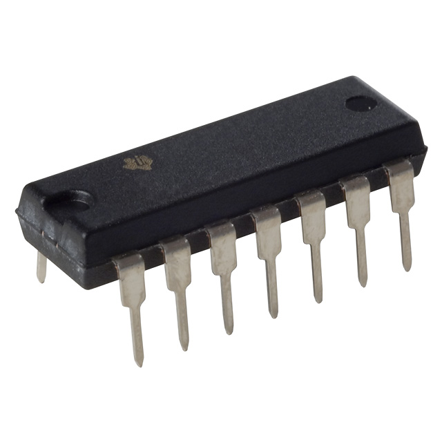
Want to post a buying lead? If you are not a member yet, please select the specific/related part number first and then fill the quantity and your contact details in the "Request for Quotation Form" on the left, and then click "Send RFQ".Your buying lead can then be posted, and the reliable suppliers will quote via our online message system or other channels soon.
Quality, low-cost, bipolar fabrication with innovative design concepts is employed for the TL3474, TL3474A operational amplifiers. These devices offer 4 MHz of gain-bandwidth product, 13-V/s slew rate, and fast settling time without the use of JFET device technology. Although the TL3474 and TL3474A can be operated from split supplies, they are particularly suited for single-supply operation because the common-mode input voltage range includes ground potential (VCC−). With a Darlington transistor input stage, these devices exhibit high input resistance, low input offset voltage, and high gain. The all-npn output stage, characterized by no dead-band crossover distortion and large output voltage swing, provides high-capacitance drive capability, excellent phase and gain margins, low open-loop high-frequency output impedance, and symmetrical source/sink ac frequency response. These low-cost amplifiers are an alternative to the MC34074/A and MC33074/A operational amplifiers.
TL3474ACN Maximum Ratings
Supply voltage: VCC+ (see Note 1).. . . . . . . . 18 V VCC−.. . . . . . . . . . . . . . . . . . −18 V Differential input voltage, VID (see Note 2). .±36 V Input voltage, VI (any input).. . . . . . . . . . . . . VCC± Input current, II (each input).. . . . . . . . . . . .±1 mA Output current, IO.. . . . . . . . . . . . . . . . . . .±80 mA Total current into VCC+.. . . . . . . . . . . . . . . . .80 mA Total current out of VCC−.. . . . . . . . . . . . . . . 80 mA Duration of short-circuit current at (or below) 25 (see Note 3). . . . . Unlimited Package thermal impedance, JA (see Notes 4 and 5): D package. . . 86/W N package. . . . . . . . . . . ..80/W PW package. . . . . . .. . . .113/W Operating virtual junction temperature, TJ. . . . . . . . . . . . .150 Lead temperature 1.6 mm (1/16 inch) from case for 10 seconds. . . . . . 260 Storage temperature range, Tstg.. .. . . . . . . . . . .−65 to 150
† Stresses beyond those listed under "absolute maximum ratings" may cause permanent damage to the device. These are stress ratings only, and functional operation of the device at these or any other conditions beyond those indicated under "recommended operating conditions" is not implied. Exposure to absolute-maximum-rated conditions for extended periods may affect device reliability.
NOTES: 1. All voltage values, except differential voltages, are with respect to the midpoint between VCC+ and VCC−/GND. 2. Differential voltages are at the noninverting input with respect to the inverting input. Excessive input current can flow when the input is less than VCC− − 0.3 V. 3. The output can be shorted to either supply. Temperature and/or supply voltages must be limited to ensure that the maximum dissipation rating is not exceeded. 4. Maximum power dissipation is a function of TJ(max), JA, and TA. The maximum allowable power dissipation at any allowable ambient temperature is PD = (TJ(max) − TA)/JA. Operating at the absolute maximum TJ of 150 can affect reliability. 5. The package thermal impedance is calculated in accordance with JESD 51-7.
TL3474ACN Features
` Low Offset . . . 3 mV (Max) for A-Grade ` Wide Gain-Bandwidth Product . . . 4 MHz ` High Slew Rate . . . 13 V/s ` Fast Settling Time . . . 1.1 s to 0.1% ` Wide-Range Single-Supply Operation. . . 4 V to 36 V ` Wide Input Common-Mode Range Includes Ground (VCC−) ` Low Total Harmonic Distortion . . . 0.02% ` Large-Capacitance Drive Capability . . . 10,000 pF ` Output Short-Circuit Protection ` Alternative to MC33074/A and MC34074/A
TL3474ACN Connection Diagram
TL3474ACPW Parameters
Technical/Catalog Information
TL3474ACPW
Vendor
Texas Instruments
Category
Integrated Circuits (ICs)
Packaging
Tube
Amplifier Type
General Purpose
Number of Circuits
4 - Quad
Package / Case
14-TSSOP
Slew Rate
13 V/s
Gain Bandwidth Product
4MHz
Current - Supply
3.5mA
Current - Output / Channel
34mA
Voltage - Supply, Single/Dual (±)
4 V ~ 36 V, ±2 V ~ 18 V
Output Type
-
-3db Bandwidth
-
Current - Input Bias
100nA
Operating Temperature
0°C ~ 70°C
Voltage - Input Offset
1000V
Drawing Number
296; 4040064; PW; 8, 14, 16, 20, 24, 28
Lead Free Status
Lead Free
RoHS Status
RoHS Compliant
Other Names
TL3474ACPW TL3474ACPW
TL3474ACPW General Description
Quality, low-cost, bipolar fabrication with innovative design concepts is employed for the TL3474, TL3474A operational amplifiers. These devices offer 4 MHz of gain-bandwidth product, 13-V/s slew rate, and fast settling time without the use of JFET device technology. Although the TL3474 and TL3474A can be operated from split supplies, they are particularly suited for single-supply operation because the common-mode input voltage range includes ground potential (VCC−). With a Darlington transistor input stage, these devices exhibit high input resistance, low input offset voltage, and high gain. The all-npn output stage, characterized by no dead-band crossover distortion and large output voltage swing, provides high-capacitance drive capability, excellent phase and gain margins, low open-loop high-frequency output impedance, and symmetrical source/sink ac frequency response. These low-cost amplifiers are an alternative to the MC34074/A and MC33074/A operational amplifiers.
TL3474ACPW Maximum Ratings
Supply voltage: VCC+ (see Note 1).. . . . . . . . 18 V VCC−.. . . . . . . . . . . . . . . . . . −18 V Differential input voltage, VID (see Note 2). .±36 V Input voltage, VI (any input).. . . . . . . . . . . . . VCC± Input current, II (each input).. . . . . . . . . . . .±1 mA Output current, IO.. . . . . . . . . . . . . . . . . . .±80 mA Total current into VCC+.. . . . . . . . . . . . . . . . .80 mA Total current out of VCC−.. . . . . . . . . . . . . . . 80 mA Duration of short-circuit current at (or below) 25 (see Note 3). . . . . Unlimited Package thermal impedance, JA (see Notes 4 and 5): D package. . . 86/W N package. . . . . . . . . . . ..80/W PW package. . . . . . .. . . .113/W Operating virtual junction temperature, TJ. . . . . . . . . . . . .150 Lead temperature 1.6 mm (1/16 inch) from case for 10 seconds. . . . . . 260 Storage temperature range, Tstg.. .. . . . . . . . . . .−65 to 150
† Stresses beyond those listed under "absolute maximum ratings" may cause permanent damage to the device. These are stress ratings only, and functional operation of the device at these or any other conditions beyond those indicated under "recommended operating conditions" is not implied. Exposure to absolute-maximum-rated conditions for extended periods may affect device reliability.
NOTES: 1. All voltage values, except differential voltages, are with respect to the midpoint between VCC+ and VCC−/GND. 2. Differential voltages are at the noninverting input with respect to the inverting input. Excessive input current can flow when the input is less than VCC− − 0.3 V. 3. The output can be shorted to either supply. Temperature and/or supply voltages must be limited to ensure that the maximum dissipation rating is not exceeded. 4. Maximum power dissipation is a function of TJ(max), JA, and TA. The maximum allowable power dissipation at any allowable ambient temperature is PD = (TJ(max) − TA)/JA. Operating at the absolute maximum TJ of 150 can affect reliability. 5. The package thermal impedance is calculated in accordance with JESD 51-7.
TL3474ACPW Features
` Low Offset . . . 3 mV (Max) for A-Grade ` Wide Gain-Bandwidth Product . . . 4 MHz ` High Slew Rate . . . 13 V/s ` Fast Settling Time . . . 1.1 s to 0.1% ` Wide-Range Single-Supply Operation. . . 4 V to 36 V ` Wide Input Common-Mode Range Includes Ground (VCC−) ` Low Total Harmonic Distortion . . . 0.02% ` Large-Capacitance Drive Capability . . . 10,000 pF ` Output Short-Circuit Protection ` Alternative to MC33074/A and MC34074/A