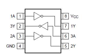
TC7WG04FK, TC7WG04FU, TC7WG08FC Selling Leads, Datasheet
MFG:TOSHIBA Package Cooled:US-9 D/C:2008+

TC7WG04FK, TC7WG04FU, TC7WG08FC Datasheet download

Part Number: TC7WG04FK
MFG: TOSHIBA
Package Cooled: US-9
D/C: 2008+


MFG:TOSHIBA Package Cooled:US-9 D/C:2008+

TC7WG04FK, TC7WG04FU, TC7WG08FC Datasheet download

MFG: TOSHIBA
Package Cooled: US-9
D/C: 2008+
Want to post a buying lead? If you are not a member yet, please select the specific/related part number first and then fill the quantity and your contact details in the "Request for Quotation Form" on the left, and then click "Send RFQ".Your buying lead can then be posted, and the reliable suppliers will quote via our online message system or other channels soon.
TOP
PDF/DataSheet Download
Datasheet: TC7WG04FK
File Size: 201003 KB
Manufacturer: TOSHIBA [Toshiba Semiconductor]
Download : Click here to Download
PDF/DataSheet Download
Datasheet: TC7WG04FU
File Size: 201003 KB
Manufacturer: TOSHIBA [Toshiba Semiconductor]
Download : Click here to Download
PDF/DataSheet Download
Datasheet: TC70
File Size: 92092 KB
Manufacturer: TELCOM [TelCom Semiconductor, Inc]
Download : Click here to Download
| Characteristics | Symbol | Ratingh | Unit |
| Power supply viltage | VCC | −0.5~4.6 | V |
| DC input voltage | VIN | −0.5~7.0 | V |
| DC output voltage | VOUT | −0.5~4.6 (Note 1) | V |
| −0.5~VCC + 0.5 (Note 2) | |||
| Input diode current | IIK | −20 | mA |
| Output diode current | IOK | −20 (Note 3) | mA |
| DC output current | IOUT | ±25 | mA |
| DC VCC/GND current | ICC | ±50 | mA |
| Power dissipation | PD | 300 (SM8) 200 (US8) |
mW |
| Storage temperature | Tstg | −65~150 | °C |
Note: Using continuously under heavy loads (e.g. the application of high temperature/current/voltage and the significant change in temperature, etc.) may cause this product to decrease in the reliability significantly even if the operating conditions (i.e. operating temperature/current/voltage, etc.) are within the absolute maximum ratings and the operating ranges. Please design the appropriate reliability upon reviewing the Toshiba Semiconductor Reliability Handbook ("Handling Precautions"/Derating Concept and Methods) and individual reliability data (i.e. reliability test report and estimated failure rate, etc).
Note 1: VCC = 0V
Note 2: High or Low State. IOUT absolute maximum rating must be observed.
Note 3: VOUT < GND

| Characteristic |
Symbol |
Value |
Unit |
| Power supply voltage |
VCC |
−0.5~4.6 |
V |
| DC input voltage |
VIN |
−0.5~7.0 |
V |
| DC output voltage |
VOUT |
−0.5~4.6 (Note 1) −0.5~VCC + 0.5 (Note 2) |
V |
| Input diode current |
IIK |
−20 |
mA |
| Output diode current |
IOK |
−20 (Note 3) |
mA |
| DC output current |
IOUT |
±25 |
mA |
| DC VCC/GND current |
ICC |
±50 |
mA |
| Power dissipation |
PD |
150 (Note 4) |
mW |
| Storage temperature |
Tstg |
−65~150 |
Note: Using continuously under heavy loads (e.g. the application of high temperature/current/voltage and the significant change in temperature, etc.) may cause this product to decrease in the reliability significantly even if the operating conditions (i.e. operating temperature/current/voltage, etc.) are within the absolute maximum ratings and the operating ranges. Please design the appropriate reliability upon reviewing the Toshiba Semiconductor Reliability Handbook ("Handling Precautions"/Derating Concept and Methods) and individual reliability data (i.e. reliability test report and estimated failure rate, etc).
Note 1: VCC = 0V
Note 2: High or Low State. IOUT absolute maximum rating must be observed.
Note 3: VOUT < GND Note 4: Mounted on an FR4 board. (25.4 mm * 25.4 mm * 1.6 t, Cu Pad: 11.56 mm2)
