TC74AC166AF, TC74AC166FN, TC74AC174AF Selling Leads, Datasheet
MFG:TOS Package Cooled:06+ D/C:96

TC74AC166AF, TC74AC166FN, TC74AC174AF Datasheet download

Part Number: TC74AC166AF
MFG: TOS
Package Cooled: 06+
D/C: 96


MFG:TOS Package Cooled:06+ D/C:96

TC74AC166AF, TC74AC166FN, TC74AC174AF Datasheet download

MFG: TOS
Package Cooled: 06+
D/C: 96
Want to post a buying lead? If you are not a member yet, please select the specific/related part number first and then fill the quantity and your contact details in the "Request for Quotation Form" on the left, and then click "Send RFQ".Your buying lead can then be posted, and the reliable suppliers will quote via our online message system or other channels soon.
TOP
PDF/DataSheet Download
Datasheet: TC70
File Size: 92092 KB
Manufacturer: TELCOM [TelCom Semiconductor, Inc]
Download : Click here to Download
PDF/DataSheet Download
Datasheet: TC74AC166FN
File Size: 320767 KB
Manufacturer: Toshiba
Download : Click here to Download
PDF/DataSheet Download
Datasheet: TC70
File Size: 92092 KB
Manufacturer: TELCOM [TelCom Semiconductor, Inc]
Download : Click here to Download
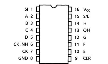
The TC74AC166 is an advanced high speed CMOS 8-BIT PARALLEL/SERIAL-IN, SERIAL-OUT SHIFT REGISTER fabricated with silicon gate and double-layer metal wiring C2MOS technology.
It achieves the high speed operation similar to equivalent Bipolar Schottky TTL while maintaining the CMOS low power dissipation.
It consists of parallel-in or serial-in, serial-out 8-bit shift register with a gated clock input and an overriding clear input. The parallel-in or serial-in modes are controlled by the SHIFT/ LOAD input. When the SHIFT/ LOAD input is held high, the serial data input is enabled and the eight flip-flops perform serial shifting on each clock pulse. When held low, the parallel data inputs are enabled and synchronous loading occurs on the next clock pulse. Clocking is accomplished on the low-to-high transition of the clock pulse. The CLOCK-INHIBIT input should be shifted high only while the CLOCK input is held high. A direct clear input overrides all other inputs, including the clock, and sets all the flip-flops to zero. Functional details are shown in the truth table and the timing charts.
All inputs are equipped with protection circuits against static discharge or transient excess voltage.
|
Characteristics |
Symbol |
Rating |
Unit |
| Supply voltage range |
VCC |
−0.5 to 7.0 |
V |
| DC input voltage |
VIN |
−0.5 to VCC + 0.5 |
V |
| DC output voltage |
VOUT |
−0.5 to VCC + 0.5 |
V |
| Input diode current |
IIK |
±20 |
mA |
| Output diode current |
IOK |
±50 |
mA |
| DC output current |
IOUT |
±50 |
mA |
| DC VCC/ground current |
ICC |
±100 |
mA |
| Power dissipation |
PD |
500 (DIP) (Note 2)/180 (SOP) |
mW |
| Storage temperature |
Tstg |
−65 to 150 |
Note 1: Exceeding any of the absolute maximum ratings, even briefly, lead to deterioration in IC performance or even destruction.
Using continuously under heavy loads (e.g. the application of high temperature/current/voltage and the significant change in temperature, etc.) may cause this product to decrease in the reliability significantly even if the operating conditions (i.e. operating temperature/current/voltage, etc.) are within the absolute maximum ratings and the operating ranges.
Please design the appropriate reliability upon reviewing the Toshiba Semiconductor Reliability Handbook ("Handling Precautions"/Derating Concept and Methods) and individual reliability data (i.e. reliability test report and estimated failure rate, etc).
Note 2: 500 mW in the range of Ta = −40 to 65 . From Ta = 65 to 85 a derating factor of −10 mW/ should be applied up to 300 mW.

