Want to post a buying lead? If you are not a member yet, please select the specific/related part number first and then fill the quantity and your contact details in the "Request for Quotation Form" on the left, and then click "Send RFQ".Your buying lead can then be posted, and the reliable suppliers will quote via our online message system or other channels soon.
The TC1411/1411N are 1A CMOS buffer/drivers. They will not latch up under any conditions within their power and voltage ratings. They are not subject to damage when up to 5V of noise spiking of either polarity occurs on the ground pin. They can accept, without damage or logic upset, up to 500 mA of current of either polarity being forced back into their output. All terminals are fully protected against up to 4 kV of electrostatic discharge.
As MOSFET drivers, the TC1411/1411N can easily switch 1000 pF gate capacitance in 25nsec with matched rise and fall times, and provide low enough impedance in both the ON and the OFF states to ensure the MOSFET's intended state will not be affected, even by large transients. The rise and fall time edges are matched to allow driving short-duration inputs with greater accuracy.
TC1411EOA Maximum Ratings
Supply Voltage ......................................................... +20V Input Voltage, IN A or IN B ..(VDD + 0.3V) to (GND 5.0V) Maximum Chip Temperature................................. +150°C Storage Temperature Range ............... 65°C to +150°C Lead Temperature (Soldering, 10 sec) ................ +300°C Package Thermal Resistance CerDIP RJ-A ............................................... 150°C/W CerDIP RJ-C ................................................. 50°C/W PDIP RJ-A ................................................... 125°C/W PDIP RJ-C .................................................... 42°C/W SOIC RJ-A .................................................. 155°C/W SOIC RJ-C .................................................... 45°C/W Operating Temperature Range C Version ............................................ 0°C to +70°C E Version ....................................... 40°C to +85°C Power Dissipation (TA 70°C) Plastic .............................................................730mW CerDIP ............................................................800mW SOIC ...............................................................470mW
TC1411EOA Features
Latch-Up Protected: Will Withstand 500mA Reverse Current Input Will Withstand Negative Inputs Up to 5V ESD Protected ....................................................4 kV High Peak Output Current .................................. 1A Wide Operating Range .......................... 4.5V to 16V High Capacitive Load Drive Capability .......................... 1000pF in 25nsec Short Delay Time .................................. 30nsec Typ Consistent Delay Times With Changes in Supply Voltage Matched Delay Times Low Supply Current - With Logic "1" Input ................................. 500A - With Logic "0" Input ................................. 150A Low Output Impedance ....................................... 8 Pinout Same as TC1410/12/13
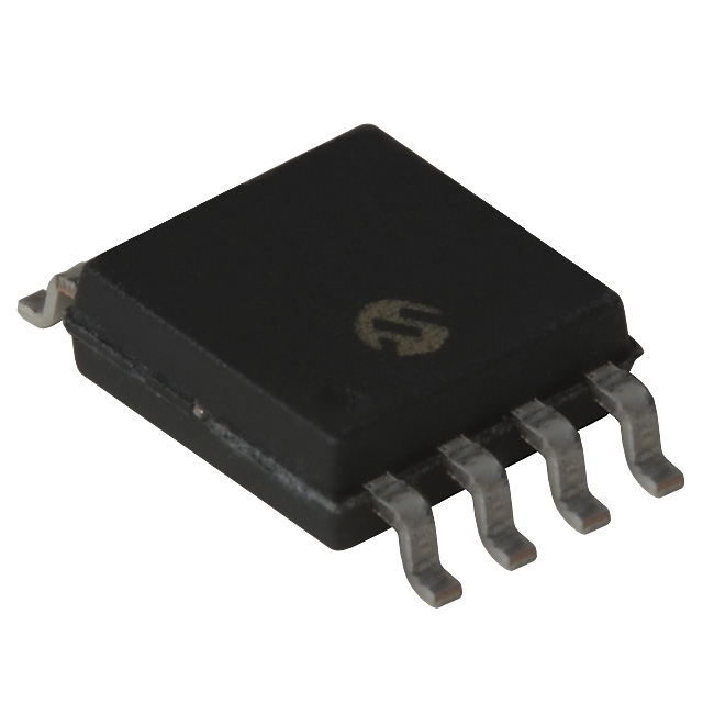
TC1411EOA Connection Diagram
TC1411EOA713 Parameters
Technical/Catalog Information
TC1411EOA713
Vendor
Microchip Technology
Category
Integrated Circuits (ICs)
Configuration
Low-Side
Voltage - Supply
4.5 V ~ 16 V
Current - Peak
1A
Delay Time
30ns
Package / Case
8-SOIC (3.9mm Width)
Packaging
Tape & Reel (TR)
Number of Outputs
1
Input Type
Inverting
Number of Configurations
1
Operating Temperature
-40°C ~ 85°C
High Side Voltage - Max (Bootstrap)
-
Lead Free Status
Lead Free
RoHS Status
RoHS Compliant
Other Names
TC1411EOA713 TC1411EOA713
TC1411EPA Parameters
Technical/Catalog Information
TC1411EPA
Vendor
Microchip Technology
Category
Integrated Circuits (ICs)
Configuration
Low-Side
Voltage - Supply
4.5 V ~ 16 V
Current - Peak
1A
Delay Time
30ns
Package / Case
8-DIP (300 mil)
Packaging
Tube
Number of Outputs
1
Input Type
Inverting
Number of Configurations
1
Operating Temperature
-40°C ~ 85°C
High Side Voltage - Max (Bootstrap)
-
Lead Free Status
Lead Free
RoHS Status
RoHS Compliant
Other Names
TC1411EPA TC1411EPA
TC1411EPA General Description
The TC1411/1411N are 1A CMOS buffer/drivers. They will not latch up under any conditions within their power and voltage ratings. They are not subject to damage when up to 5V of noise spiking of either polarity occurs on the ground pin. They can accept, without damage or logic upset, up to 500 mA of current of either polarity being forced back into their output. All terminals are fully protected against up to 4 kV of electrostatic discharge.
As MOSFET drivers, the TC1411/1411N can easily switch 1000 pF gate capacitance in 25nsec with matched rise and fall times, and provide low enough impedance in both the ON and the OFF states to ensure the MOSFET's intended state will not be affected, even by large transients. The rise and fall time edges are matched to allow driving short-duration inputs with greater accuracy.
TC1411EPA Maximum Ratings
Supply Voltage ......................................................... +20V Input Voltage, IN A or IN B ..(VDD + 0.3V) to (GND 5.0V) Maximum Chip Temperature................................. +150°C Storage Temperature Range ............... 65°C to +150°C Lead Temperature (Soldering, 10 sec) ................ +300°C Package Thermal Resistance CerDIP RJ-A ............................................... 150°C/W CerDIP RJ-C ................................................. 50°C/W PDIP RJ-A ................................................... 125°C/W PDIP RJ-C .................................................... 42°C/W SOIC RJ-A .................................................. 155°C/W SOIC RJ-C .................................................... 45°C/W Operating Temperature Range C Version ............................................ 0°C to +70°C E Version ....................................... 40°C to +85°C Power Dissipation (TA 70°C) Plastic .............................................................730mW CerDIP ............................................................800mW SOIC ...............................................................470mW
TC1411EPA Features
Latch-Up Protected: Will Withstand 500mA Reverse Current Input Will Withstand Negative Inputs Up to 5V ESD Protected ....................................................4 kV High Peak Output Current .................................. 1A Wide Operating Range .......................... 4.5V to 16V High Capacitive Load Drive Capability .......................... 1000pF in 25nsec Short Delay Time .................................. 30nsec Typ Consistent Delay Times With Changes in Supply Voltage Matched Delay Times Low Supply Current - With Logic "1" Input ................................. 500A - With Logic "0" Input ................................. 150A Low Output Impedance ....................................... 8 Pinout Same as TC1410/12/13