T-7689-FL, T7690, T7690FL0020T Selling Leads, Datasheet
MFG:LUCENT Package Cooled:QFP D/C:0048

T-7689-FL, T7690, T7690FL0020T Datasheet download

Part Number: T-7689-FL
MFG: LUCENT
Package Cooled: QFP
D/C: 0048


MFG:LUCENT Package Cooled:QFP D/C:0048

T-7689-FL, T7690, T7690FL0020T Datasheet download

MFG: LUCENT
Package Cooled: QFP
D/C: 0048
Want to post a buying lead? If you are not a member yet, please select the specific/related part number first and then fill the quantity and your contact details in the "Request for Quotation Form" on the left, and then click "Send RFQ".Your buying lead can then be posted, and the reliable suppliers will quote via our online message system or other channels soon.
TOP
PDF/DataSheet Download
Datasheet: T-7290
File Size: 1404336 KB
Manufacturer: ETC [ETC]
Download : Click here to Download
PDF/DataSheet Download
Datasheet: T7690
File Size: 743523 KB
Manufacturer: Lucent Technologies
Download : Click here to Download
PDF/DataSheet Download
Datasheet: T7600130
File Size: 164540 KB
Manufacturer: POWEREX [Powerex Power Semiconductors]
Download : Click here to Download
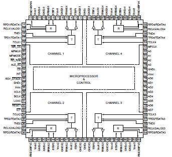
The T7690 and T7693 are fully integrated quad line interfaces containing four transmit and receive channels for use in both North American (T1/DS1) and European (E1/CEPT) applications. The devices have many of the same functions as the Lucent Technologies Microelectronics Group T7290A and provide additional flexibility for the system designer.
Included is a parallel microprocessor interface that allows the user to define the architecture, initiate loopbacks, and monitor alarms. The interface is compatible with many commercially available microprocessors.
The receiver performs clock and data recovery using a fully integrated digital phase-locked loop. This digital implementation prevents false lock conditions that are common when recovering sparse data patterns with analog phase-locked loops. Equalization circuitry in the receiver guarantees a high level of interference immunity. As an option, the raw sliced data (no retiming) can be output on the receive data pins.
Transmit equalization is implemented with lowimpedance output drivers that provide shaped waveforms to the transformer, guaranteeing template conformance. The quad device will interface to the digital cross connect (DSX) at lengths of up to 655 ft. for DS1 operation or to line impedances of 75 or 120 for CEPT operation.
A selectable jitter attenuator may be placed in the receive signal path for low-bandwidth line-synchronous applications, or it may be placed in the transmit path for multiplexer applications where DS1/CEPT signals are demultiplexed from higher rate signals. The jitter attenuator will perform the clock smoothing required on the resulting demultiplexed gapped clock.
| Parameter |
Min |
Max |
Unit |
| dc Supply Voltage |
-0.5 |
6.5 |
V |
| Storage Temperature |
-65 |
125 |
|
| Maximum Voltage (digital pins) with Respect to VDDD |
- |
0.5 |
V |
| Minimum Voltage (digital pins) with Respect to GNDD |
-0.5 |
- |
V |
| Maximum Allowable Voltages (RTIP[1-4], RRING[1-4]) with Respect to VDD |
- |
0.5 |
V |
| Minimum Allowable Voltages (RTIP[1-4], RRING[1-4]) with Respect to GND |
-0.5 |
- |
V |

