SC111CH004-SX, SC111OTS, SC112 Selling Leads, Datasheet
MFG:N/A D/C:05.08

SC111CH004-SX, SC111OTS, SC112 Datasheet download

Part Number: SC111CH004-SX
MFG: N/A
Package Cooled:
D/C: 05.08


MFG:N/A D/C:05.08
SC111CH004-SX, SC111OTS, SC112 Datasheet download
MFG: N/A
Package Cooled:
D/C: 05.08

Want to post a buying lead? If you are not a member yet, please select the specific/related part number first and then fill the quantity and your contact details in the "Request for Quotation Form" on the left, and then click "Send RFQ".Your buying lead can then be posted, and the reliable suppliers will quote via our online message system or other channels soon.
TOP
PDF/DataSheet Download
Datasheet: SC100
File Size: 2737062 KB
Manufacturer: Motorola, Inc
Download : Click here to Download
PDF/DataSheet Download
Datasheet: SC100
File Size: 2737062 KB
Manufacturer: Motorola, Inc
Download : Click here to Download
PDF/DataSheet Download
Datasheet: SC112
File Size: 60126 KB
Manufacturer: SEMTECH [Semtech Corporation]
Download : Click here to Download
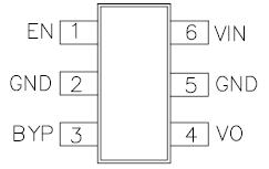
The SC112 is a 150mA ultra low dropout linear regulator with a built in CMOS/TTL logic level enable, designed specifically for battery powered applications where low quiescent current and low dropout are critical for battery longevity.
The SC112 uses a Semtech proprietary internal PNP device for the pass element, providing a low dropout voltage of 130mV at a load of 60mA.
The output noise is reduced to 30V (typical) by placing a very low leakage 10nF capacitor on pin 3 (noise bypass).
Each device contains a bandgap reference, error amplifier, PNP pass element, thermal and current limiting circuitry and resistor divider network for setting output voltage.
The SC112 is packaged in a six lead SOT-23 surface mount package for a very small footprint and it requires only a 1F capacitor on the output and a 0.01F on the bypass pin for a minimum number of external components.
| Parameter | Symbol | Maximum | Units |
| Input Supply Voltage | VIN | -0.3 to 16 | V |
| Enable Input Voltage | VEN | -0.3 to VIN | V |
| Power Dissipation | Pd | Internally Limited | W |
| Thermal Resistance Junction to Ambient | JA | 230 | °C/W |
| Operating Ambient Temperature Range | TA | -40 to +85 | °C |
| Operating Junction Temperature Range | TA | -40 to +125 | °C |
| Storage Temperature Range | TSTG | -55 to +150 | °C |
| Lead Temperature (Soldering) 10 Sec | TLEAD | 300 | °C |
| ESD Rating (Human | ESD | 2 | kV |
• Low dropout voltage
• CMOS/TTL compatible control switch
• Very low quiescent current 60A (ON, no load)
• Internal thermal shutdown
• Short circuit protection
• Very low standby current 0.1A maximum (OFF)
• Low noise with external bypass capacitor
• Industrial temperature range
• Battery powered systems
• Cellular telephones
• Cordless telephones
• Pagers, personal digital assistants
• Portable instrumentation
• Low voltage systems

Price: 4-6 USD
MT58L64L18CT-10 TQFP100

Price: 5-6.5 USD
DL-7140-211M laser tube

Price: 4-5 USD
74LVC74APG - IC FLIP FLOP D-Type POS-EDG DUAL 14TSSOP

Price: 6.5-8 USD
CYPRESS - Clock Synthesizer with Differential CPU Outputs

Price: 0.284-0.286 USD
PI5V330QEX Pericom Multiplexer Switch ICs

Price: 1-2 USD
IGBT power module, Single switch, 1200 V, Collector-emitter voltage, 430A

Price: 1-2 USD
a-Si TFT-LCD, NEC, 228.096Hmm, 560V

Price: 0.124-0.2 USD
PC354N1T - Mini-flat Package, AC Input Type Photocoupler - Sharp Electrionic Components

Price: 0.177-0.178 USD
RL1210JR51-XX-BL - Thick Film Chip Resistor Low Ohmic - TAITRON Components Incorporated

Price: 0.053-0.055 USD
STPS140A - POWER SCHOTTKY RECTIFIER - STMicroelectronics

Price: 1.45-1.5 USD
STA013 - MPEG 2.5 LAYER III AUDIO DECODER - STMicroelectronics

Price: 0.073-0.075 USD
SMBJ5347B - 5 Watt Surface Mount Silicon Zener Diodes - Micro Commercial Components
