PLS169AN, PLS173, PLS173/BLA(5962-8850402LA) Selling Leads, Datasheet
MFG:SIEMENS Package Cooled:DIP D/C:90

PLS169AN, PLS173, PLS173/BLA(5962-8850402LA) Datasheet download

Part Number: PLS169AN
MFG: SIEMENS
Package Cooled: DIP
D/C: 90


MFG:SIEMENS Package Cooled:DIP D/C:90
PLS169AN, PLS173, PLS173/BLA(5962-8850402LA) Datasheet download
MFG: SIEMENS
Package Cooled: DIP
D/C: 90

Want to post a buying lead? If you are not a member yet, please select the specific/related part number first and then fill the quantity and your contact details in the "Request for Quotation Form" on the left, and then click "Send RFQ".Your buying lead can then be posted, and the reliable suppliers will quote via our online message system or other channels soon.
TOP
PDF/DataSheet Download
Datasheet: PLS1
File Size: 84159 KB
Manufacturer:
Download : Click here to Download
PDF/DataSheet Download
Datasheet: PLS173
File Size: 75262 KB
Manufacturer: PHILIPS [Philips Semiconductors]
Download : Click here to Download
PDF/DataSheet Download
Datasheet: PLS1
File Size: 84159 KB
Manufacturer:
Download : Click here to Download
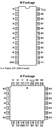
The PLS173 is a two-level logic element consisting of 42 AND gates and 10 OR gates with fusible link connections for programming I/O polarity and direction.
All AND gates are linked to 12 inputs (I) and 10 bidirectional I/O lines (B). These yield variable I/O gate configurations via 10 direction control gates (D), ranging from 22 inputs to 10 outputs.
On-chip T/C buffers couple either True (I, B) or Complement (I, B) input polarities to all AND gates, whose outputs can be optionally linked to all OR gates. Their output polarity, in turn, is individually programmable through a set of EX-OR gates for implementing AND/OR or AND/NOR logic functions.
The PLS173 is field programmable, enabling the user to quickly generate custom patterns using standard programming equipment.
Order codes for this device are listed below.
|
SYMBOL |
PARAMETER |
RATING |
UNIT | |
|
MIN. |
MAX. | |||
|
VCC |
Supply voltage |
+7 |
VDC | |
|
VIN |
Input voltage |
+5.5 |
VDC | |
|
VOUT |
Output voltage |
+5.5 |
VDC | |
|
IIN |
Input currents |
-30 |
+30 |
nA |
|
IOUT |
Output currents |
+100 |
mA | |
|
TAMB |
Operating free-air temperature range |
0 |
+75 |
|
|
TSTG |
Storage temperature range |
-65 |
+150 |
|
NOTES:
1. Stresses above those listed may cause malfunction or permanent damage to the device. This is a stress rating only. Functional operation at these or any other condition above those indicated in the operational and programming specification of the device is not implied.
Note
1. Up to 0.3 mm from ceramic.

Price: 4-6 USD
MT58L64L18CT-10 TQFP100

Price: 5-6.5 USD
DL-7140-211M laser tube

Price: 4-5 USD
74LVC74APG - IC FLIP FLOP D-Type POS-EDG DUAL 14TSSOP

Price: 6.5-8 USD
CYPRESS - Clock Synthesizer with Differential CPU Outputs

Price: 0.284-0.286 USD
PI5V330QEX Pericom Multiplexer Switch ICs

Price: 1-2 USD
IGBT power module, Single switch, 1200 V, Collector-emitter voltage, 430A

Price: 1-2 USD
a-Si TFT-LCD, NEC, 228.096Hmm, 560V

Price: 0.124-0.2 USD
PC354N1T - Mini-flat Package, AC Input Type Photocoupler - Sharp Electrionic Components

Price: 0.177-0.178 USD
RL1210JR51-XX-BL - Thick Film Chip Resistor Low Ohmic - TAITRON Components Incorporated

Price: 0.053-0.055 USD
STPS140A - POWER SCHOTTKY RECTIFIER - STMicroelectronics

Price: 1.45-1.5 USD
STA013 - MPEG 2.5 LAYER III AUDIO DECODER - STMicroelectronics

Price: 0.073-0.075 USD
SMBJ5347B - 5 Watt Surface Mount Silicon Zener Diodes - Micro Commercial Components
