MM74C89, MM74C89J, MM74C902J/883 Selling Leads, Datasheet
MFG:200 Package Cooled:NS D/C:DIP

MM74C89, MM74C89J, MM74C902J/883 Datasheet download

Part Number: MM74C89
MFG: 200
Package Cooled: NS
D/C: DIP


MFG:200 Package Cooled:NS D/C:DIP
MM74C89, MM74C89J, MM74C902J/883 Datasheet download
MFG: 200
Package Cooled: NS
D/C: DIP

Want to post a buying lead? If you are not a member yet, please select the specific/related part number first and then fill the quantity and your contact details in the "Request for Quotation Form" on the left, and then click "Send RFQ".Your buying lead can then be posted, and the reliable suppliers will quote via our online message system or other channels soon.
TOP
PDF/DataSheet Download
Datasheet: MM74C89
File Size: 62106 KB
Manufacturer: FAIRCHILD [Fairchild Semiconductor]
Download : Click here to Download
PDF/DataSheet Download
Datasheet: MM74C89J
File Size: 133305 KB
Manufacturer: NSC [National Semiconductor]
Download : Click here to Download
PDF/DataSheet Download
Datasheet: MM70C95
File Size: 163181 KB
Manufacturer: NSC [National Semiconductor]
Download : Click here to Download
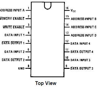
The MM74C89 is a 16-word by 4-bit random access read/write memory. Inputs to the memory consist of four address lines, four data input lines, a write enable line and a memory enable line. The four binary address inputs are decoded internally to select each of the 16 possible word locations. An internal address register latches the address information on the positive to negative transition of the memory enable input. The four 3-STATE data output lines working in conjunction with the memory enable input provide for easy memory expansion.
Address Operation: Address inputs must be stable tSA prior to the positive to negative transition of memory enable. It is thus not necessary to hold address information stable for more than tHA after the memory is enabled (positive to negative transition of memory enable).
Write Operation: Information present at the data inputs is written into the memory at the selected address by bringing write enable and memory enable LOW.
| Voltage at Any Pin |
-0.3V to VCC + 0.3V |
| Operating Temperature Range |
-40 to +85 |
| Storage Temperature Range (TS) |
-65 to +150 |
| Power Dissipation (PD) | |
| Dual-In-Line |
700 mW |
| Small Outline |
500 mW |
| Operating VCC Range |
3.0V to 15V |
| Absolute Maximum VCC |
18V |
| Lead Temperature (TL) | |
| (Soldering, 10 seconds) |
260 |
· Wide supply voltage range: 3.0V to 15V
· Guaranteed noise margin: 1.0V
· High noise immunity: 0.45 VCC (typ.)
· Low power TTL compatibility: fan out of 2 driving 74L
· Low power consumption: 100 nW/package (typ.)
· Fast access time: 130 ns (typ.) at VCC = 10V
· 3-STATE output

Price: 4-6 USD
MT58L64L18CT-10 TQFP100

Price: 5-6.5 USD
DL-7140-211M laser tube

Price: 4-5 USD
74LVC74APG - IC FLIP FLOP D-Type POS-EDG DUAL 14TSSOP

Price: 6.5-8 USD
CYPRESS - Clock Synthesizer with Differential CPU Outputs

Price: 0.284-0.286 USD
PI5V330QEX Pericom Multiplexer Switch ICs

Price: 1-2 USD
IGBT power module, Single switch, 1200 V, Collector-emitter voltage, 430A

Price: 1-2 USD
a-Si TFT-LCD, NEC, 228.096Hmm, 560V

Price: 0.124-0.2 USD
PC354N1T - Mini-flat Package, AC Input Type Photocoupler - Sharp Electrionic Components

Price: 0.177-0.178 USD
RL1210JR51-XX-BL - Thick Film Chip Resistor Low Ohmic - TAITRON Components Incorporated

Price: 0.053-0.055 USD
STPS140A - POWER SCHOTTKY RECTIFIER - STMicroelectronics

Price: 1.45-1.5 USD
STA013 - MPEG 2.5 LAYER III AUDIO DECODER - STMicroelectronics

Price: 0.073-0.075 USD
SMBJ5347B - 5 Watt Surface Mount Silicon Zener Diodes - Micro Commercial Components
