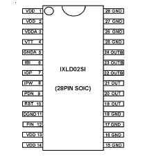
IXLD02SI, IXLD1350ET5TA, IXLD4423CPA Selling Leads, Datasheet
MFG:Ixys Package Cooled:SOP28 D/C:08+09+

IXLD02SI, IXLD1350ET5TA, IXLD4423CPA Datasheet download

Part Number: IXLD02SI
MFG: Ixys
Package Cooled: SOP28
D/C: 08+09+


MFG:Ixys Package Cooled:SOP28 D/C:08+09+

IXLD02SI, IXLD1350ET5TA, IXLD4423CPA Datasheet download

MFG: Ixys
Package Cooled: SOP28
D/C: 08+09+
Want to post a buying lead? If you are not a member yet, please select the specific/related part number first and then fill the quantity and your contact details in the "Request for Quotation Form" on the left, and then click "Send RFQ".Your buying lead can then be posted, and the reliable suppliers will quote via our online message system or other channels soon.
TOP
PDF/DataSheet Download
Datasheet:
File Size: KB
Manufacturer:
Download : Click here to Download
PDF/DataSheet Download
Datasheet:
File Size: KB
Manufacturer:
Download : Click here to Download
PDF/DataSheet Download
Datasheet:
File Size: KB
Manufacturer:
Download : Click here to Download
The IXLD02 is an ultra high-speed differential laser diode driver. The IXLD02 is designed specifically to drive single junction laser diodes in a differential fashion. A Q output and a Q-Bar output are provided via a low inductance multi-pin topology. These two signals make their transitions at the same time with transition times in the picoseconds. This technique provides the highest possible slew rate across the diode. In addition the IXLD02 is capable of currents exceeding 2A.
These performance features are combined with frequency agility to a maximum operating frequency of 17MHz, a minimum pulse width of <1.5ns and rise and fall times of approximately 600ps. In addition, the pulse width and the current programming can be modulated in real time to >10MHz. The IXLD02 is assembled in a high power SO-28 surface mount package.
For additional operational instructions, see the IXLD02 Evaluation Board application note on the DEI web site at
www.directedenergy.com
|
Name |
Definition |
Min |
Typ |
Max |
Units |
Test Conditions |
|
VDD |
Logic supply input voltage |
-0.4 |
5.5 |
V |
||
|
VDDA |
Analog bias supply input voltage |
-0.4 |
5.5 |
V |
||
|
VTT |
Internal bias voltage input |
-0.4 |
VDDA/2 |
VDDA+.5 |
V |
|
|
IBI |
Internal bias current input |
-10 |
0.1 |
10 |
mA |
|
|
VIBI |
Applied IBI terminal voltage |
-0.4 |
VDDin+0.5 |
V |
||
|
IPW |
Pulse width programming |
-10 |
0.1 |
10 |
mA |
|
|
VIPW |
Applied IPW terminal voltage |
-0.4 |
VDDin+0.5 |
V |
||
|
IOP |
Output current programming input |
-10 |
1 |
10 |
mA |
|
|
VIOP |
Applied IOP terminal voltage |
-0.4 |
VDDin+0.5 |
V |
||
|
VPDN |
Power-down logic input |
-0.4 |
VDDin+0.5 |
V |
||
|
VRST |
Reset logic input |
-0.4 |
VDDin+0.5 |
V |
||
|
VFIN |
Pulse frequency logic input |
-0.4 |
VDDin+0.5 |
V |
||
|
VOUT |
Pulse current true output |
-0.1 |
3 |
Amps |
||
|
VOUT |
OUT terminal voltage |
-0.4 |
9 |
V |
||
|
OUTB |
Pulse current complement output |
-0.1 |
3 |
Amps |
||
|
TC |
Device Case Temperature |
-40 |
25 |
85 |
Measured at the bottom of the SO28 packageheat slug insert. | |
|
PD |
Package power dissipation @ TC=85 |
32 |
Watts |
SO28 packageheat slug insert held at TC=85. | ||
|
RTHJC |
Thermal resistance, junction to case |
2 |
/W |
|||
|
TJ |
Junction Temperature |
150 |
||||
|
TS |
Storage temperature |
-55 |
150 |
|||
|
TL |
Lead temperature (soldering, 10sec) |
300 |

