IX3896GE, IX488, IX4R11 Selling Leads, Datasheet
MFG:SHARP Package Cooled:SOP D/C:96+

IX3896GE, IX488, IX4R11 Datasheet download

Part Number: IX3896GE
MFG: SHARP
Package Cooled: SOP
D/C: 96+


MFG:SHARP Package Cooled:SOP D/C:96+

IX3896GE, IX488, IX4R11 Datasheet download

MFG: SHARP
Package Cooled: SOP
D/C: 96+
Want to post a buying lead? If you are not a member yet, please select the specific/related part number first and then fill the quantity and your contact details in the "Request for Quotation Form" on the left, and then click "Send RFQ".Your buying lead can then be posted, and the reliable suppliers will quote via our online message system or other channels soon.
TOP
PDF/DataSheet Download
Datasheet:
File Size: KB
Manufacturer:
Download : Click here to Download
PDF/DataSheet Download
Datasheet: IX4R11
File Size: 630935 KB
Manufacturer: IXYS [IXYS Corporation]
Download : Click here to Download
PDF/DataSheet Download
Datasheet: IX4R11
File Size: 630935 KB
Manufacturer: IXYS [IXYS Corporation]
Download : Click here to Download
The IX4R11 Bridge Driver for N-channel MOSFETs and IGBTs with a high side and low side output, whose input signals reference the low side. The High Side driver can control a MOSFET or IGBT connected to a positive buss voltage up to 650V. The logic input stages are compatible with TTL or CMOS, have built-in hysteresis and are fully immune to latch up over the entire operating range. The IX4R11 can withstand dV/dt on the output side up to ± 50V/ns.
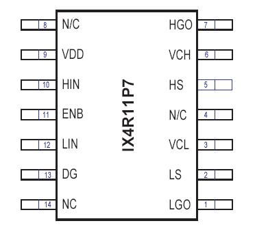
The IX4R11 comes in either the 16-PIN SOIC package (IX4R11S3) or the 14-PIN DIP through-hole package (IX4R11P7)
| Symbol | Definition | Min | Max | Units |
| VCH | High side floating supply voltage | -25 | 650 | V |
| VHS | High side floating supply offset voltage | VCH-200 | VCH+.3 | V |
| VHGO | High side floating output voltage | VHS-.3 | VCH+.3 | V |
| VCL | Low side fixed supply voltage | -0.3 | 35 | V |
| VLGO | Low side output voltage | -0.3 | VCL+.3 | V |
| VDD | Logic supply voltage | -0.3 | VDG+35 | V |
| VDG | Logic supply offset voltage | VLS-3.8 | VLS+3.8 | V |
| VIN | Logic input voltage(HIN & LIN) | VSS-.3 | VDD+.3 | V |
| dVS/dt | Allowable offset supply voltage transient | 50 | V/ns | |
| PD | Package power dissipation@ TA 25C | 1.25 | W | |
| PD | Package power dissipation@ TC 25C | 2.5 | W | |
| RTHJA | Thermal resistance, junction-to-ambient | 100 | K/W | |
| RTHJc | Thermal resistance, junction-to-case | 50 | K/W | |
| TJ | Junction Temperature | 150 | ||
| TS | Storage temperature | -55 | 150 |

