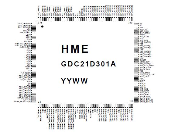
GDBJ001, GDC21D301A, GDC21D401B Selling Leads, Datasheet
MFG:ST Package Cooled:SOP-20L D/C:06+

GDBJ001, GDC21D301A, GDC21D401B Datasheet download

Part Number: GDBJ001
MFG: ST
Package Cooled: SOP-20L
D/C: 06+


MFG:ST Package Cooled:SOP-20L D/C:06+

GDBJ001, GDC21D301A, GDC21D401B Datasheet download

MFG: ST
Package Cooled: SOP-20L
D/C: 06+
Want to post a buying lead? If you are not a member yet, please select the specific/related part number first and then fill the quantity and your contact details in the "Request for Quotation Form" on the left, and then click "Send RFQ".Your buying lead can then be posted, and the reliable suppliers will quote via our online message system or other channels soon.
TOP
PDF/DataSheet Download
Datasheet:
File Size: KB
Manufacturer:
Download : Click here to Download
PDF/DataSheet Download
Datasheet: GDC21D301A
File Size: 882652 KB
Manufacturer: HYNIX [Hynix Semiconductor]
Download : Click here to Download
PDF/DataSheet Download
Datasheet: GDC21D401B
File Size: 710801 KB
Manufacturer: HYNIX [Hynix Semiconductor]
Download : Click here to Download
The GDC21D301A Transport Decoder resides in the center of an MPEG-2 decoding system. It accepts MPEG-2 transport streams, parses the transport and packetized elementary stream (PES) layers into the separate data streams, and provides rate buffering for the parsed data streams. Then it passes those data streams to video and audio decoders. The GDC21D301A also extracts Program Clock Reference (PCR) in the data stream and provides the Pulse Width
Modulation (PWM) signals in order to recover the clock and to synchronize the playback of video and audio. The GDC21D301A manages an external DRAM that is used for data storage and buffering the various parsed data streams. This DRAM is shared with the host processor so that the system's memory requirements can be consolidated into a single, low-cost DRAM. The GDC21D301A stores data packets destined for the host directly in shared DRAM for easy access by the host.
|
SYMBOL |
PARAMETERS |
VALUES |
UNIT |
|
VDD |
Power Supply Voltage |
-0.33 to 5.5 |
V |
|
VI |
Digital Input Voltage |
-0.33 to VDD + 0.5 |
V |
|
Vo |
Digital Output Voltage |
-0.33 to VDD + 0.5 |
V |
|
Tstg |
Storage Temperature |
-55 to 125 |
`` |
|
Pd |
Power Dissipation |
1.0 |
W |
Note : Absolute Maximum Ratings means that the safety of the device cannot be guaranteed beyond these values and it doesn't imply that the device
should be operated within these limits.

The Video Decoder(VD) decodes video elementary stream of MPEG-2(ISO/ICE 13818-2)MP@HL. It supports the ATSC digital TV video standard, and can be used for the video part of the ATSC digital TV with the Transport Decoder and the VDP(Video Display Processor). Picture decoding timing can be controlled internally for A/V lip synchronization, and externally for Video Trick Mode by host microprocessor via I2C bus. The Video Decoder can extract video user data including caption from video elementary stream, and host microprocessor can read the video user data from the Video Decoder(VD) via I2C. It uses four 16x1M SDRAMs and can support up to 81 MHz memory clock speed.
|
SYMBOL |
PARAMETERS |
VALUES |
UNIT |
|
VDD |
Power Supply Voltage |
-0.33 to 5.5 |
V |
|
VI |
Digital Input Voltage |
-0.33 to VDD + 0.5 |
V |
|
Vo |
Digital Output Voltage |
-0.33 to VDD + 0.5 |
V |
|
Tstg |
Storage Temperature |
-55 to 125 |
|
|
Pd |
Power Dissipation |
4.6 |
W |
*Note :Absolute Maximum Ratings mean that the safety of the device cannot be guaranteed beyond these values, and this doesn't imply that the device should be operated within these limits.

