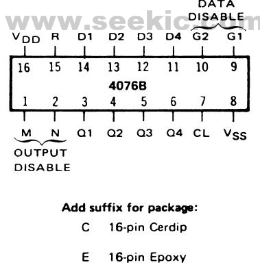
4076B, 4076BDC, 4076BDCQR Selling Leads, Datasheet
MFG:1240 Package Cooled:CDIP D/C:N/A

4076B, 4076BDC, 4076BDCQR Datasheet download

Part Number: 4076B
MFG: 1240
Package Cooled: CDIP
D/C: N/A


MFG:1240 Package Cooled:CDIP D/C:N/A

4076B, 4076BDC, 4076BDCQR Datasheet download

MFG: 1240
Package Cooled: CDIP
D/C: N/A
Want to post a buying lead? If you are not a member yet, please select the specific/related part number first and then fill the quantity and your contact details in the "Request for Quotation Form" on the left, and then click "Send RFQ".Your buying lead can then be posted, and the reliable suppliers will quote via our online message system or other channels soon.
TOP
PDF/DataSheet Download
Datasheet: 4071B
File Size: 25775 KB
Manufacturer: PHILIPS [Philips Semiconductors]
Download : Click here to Download
PDF/DataSheet Download
Datasheet: 4071B
File Size: 25775 KB
Manufacturer: PHILIPS [Philips Semiconductors]
Download : Click here to Download
PDF/DataSheet Download
Datasheet: 4071B
File Size: 25775 KB
Manufacturer: PHILIPS [Philips Semiconductors]
Download : Click here to Download
The 4076B 4-bit register is designed to consist of four D-type flip-flops operating stnchronously from a common cloce.The OR-gated output disable inputs force the outputs into a high-impedance state for use in bus-organized systems.OR-gated data disable inputs cause the Q outputs to be fed back to the D inputs of the flip-flops.Thus,they are inhibited from changing state while the clocking process remains undisturbed.To clear all four flip-flops simultaneously independent if the clock or disable inputs an asynchronous master reset is provided.
It has four features.The first one is about its 3-state outputs which would be with gated control lines.The second one is that it would have the fully independent clock.The third one is that it would have the feature of asynchronous reset.The last one is that it would have a fully static operation which means DC to to 12MHz @ 10 Vdc.
Some recommended operating conditions have been concluded into several points.For maximum reliability,The DC supply voltage which also marked as Vdd or Vss would be from 3 to 15 Vdc.Then the operating temperature,which also be marked as Ta,would be from -55 to +125°C for C and would be from -40 to 85°C for E.Also some electrical characteristics about it which is about its quiescent device current which also be marked as Idd.When Vdd(Vdc) = 5 it would have a maximum of 5 uAdc at T(low) and have a typical of 0.05 uAdc and a maximum of 5 uAdc at the room tempreture of +25°C and have a maximum of 150 uAdc at T(high). When Vdd(Vdc) = 10 it would have a maximum of 10 uAdc at T(low) and have a typical of 0.1 uAdc and a maximum of 10 uAdc at the room tempreture of +25°C and have a maximum of 300 uAdc at T(high). When Vdd(Vdc) = 15 it would have a maximum of 20 uAdc at T(low) and have a typical of 0.2 uAdc and a maximum of 20 uAdc at the room tempreture of +25°C and have a maximum of 600 uAdc at T(high).

