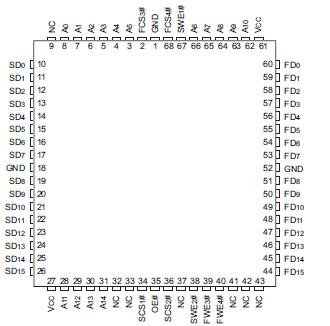
Features: ` Access Times of 35ns (SRAM) and 70ns (FLASH)` Access Times of 70ns (SRAM) and 120ns (FLASH)` Packaging • 66-pin, PGA Type, 1.075 inch square HIP,Hermetic Ceramic HIP (Package 400) • 66-pin, PGA Type, 1.185 inch square HIP,Hermetic Ceramic HIP (Package 401) • 68 lead, ...
WSF128K16-XXX: Features: ` Access Times of 35ns (SRAM) and 70ns (FLASH)` Access Times of 70ns (SRAM) and 120ns (FLASH)` Packaging • 66-pin, PGA Type, 1.075 inch square HIP,Hermetic Ceramic HIP (Package 400) ...
SeekIC Buyer Protection PLUS - newly updated for 2013!
268 Transactions
All payment methods are secure and covered by SeekIC Buyer Protection PLUS.
DescriptionThe WSF128K16-72 is designed as one kind of 128K x 32 SRAM / flash module. Features of ...
` Access Times of 35ns (SRAM) and 70ns (FLASH)
` Access Times of 70ns (SRAM) and 120ns (FLASH)
` Packaging
• 66-pin, PGA Type, 1.075 inch square HIP,Hermetic Ceramic HIP (Package 400)
• 66-pin, PGA Type, 1.185 inch square HIP,Hermetic Ceramic HIP (Package 401)
• 68 lead, Hermetic CQFP (G1U)1, 22.4mm (0.880 inch) square (Package 519). Designed to fi t JEDEC 68 lead 0.990" CQFJ footprint (FIGURE 2)
• 68 lead, Hermetic CQFP (G1T), 22.4mm (0.880 inch) square (Package 524)
` 128Kx16 SRAM
` 128Kx16 5V FLASH
` Organized as 128Kx16 of SRAM and 128Kx16 of Flash Memory with separate Data Buses
` Both blocks of memory are User Confi gurable as 256Kx8
` Low Power CMOS
` Commercial, Industrial and Military Temperature Ranges
` TTL Compatible Inputs and Outputs
` Built-in Decoupling Caps and Multiple Ground Pins for Low Noise Operation
` Weight
• WSF128K16-XHX - 13 grams typical
• WSF128K16-H1X - 13 grams typical
• WSF128K16-XG1UX1 - 5 grams typical
• WSF128K16-XG1TX - 5 grams typical
FLASH MEMORY FEATURES
` 10,000 Erase/Program Cycles
` Sector Architecture
• 8 equal size sectors of 16K bytes each
• Any combination of sectors can be concurrently erased. Also supports full chip erase
` 5 Volt Programming; 5V ± 10% Supply
` Embedded Erase and Program Algorithms
` Hardware Write Protection
` Page Program Operation and Internal Program Control Time.
Note: For programming information refer to Flash Programming 1M5 Application Note.
Note 1: Package not recommended for new designs
Parameter |
Symbol |
Min. |
Max. |
Units |
Operating Temperature |
TA |
-55 |
+125 |
|
Storage Temperature |
TSTG |
-65 |
+150 |
|
Signal Voltage Relative to GND |
VG |
-0.5 |
7.0 |
V |
Junction Temperature |
VJ |
150 |
||
Supply Voltage |
VCC |
-0.5 |
7.0 |
V |
Parameter | |
Flash Data Retention | 10 years |
Flash Endurance (write/erase cycles) | 10,000 |
NOTES: 1. Stresses above the absolute maximum rating may cause permanent damage to the device. Extended operation at the maximum levels may degrade performance and affect reliability.