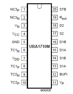
Features: · Power MOS modulators for control of GaAs power amplifier drain voltage· Power control loop amplifier and MOS driver· Voltage tripler for supply of MOS driver· Positive-to-negative DC converter for GaAs power amplifier gate biasing.Application· Control of GaAs power amplifiers for GSM a...
UBA1710M: Features: · Power MOS modulators for control of GaAs power amplifier drain voltage· Power control loop amplifier and MOS driver· Voltage tripler for supply of MOS driver· Positive-to-negative DC con...
SeekIC Buyer Protection PLUS - newly updated for 2013!
268 Transactions
All payment methods are secure and covered by SeekIC Buyer Protection PLUS.
SYMBOL |
PARAMETER |
MIN. |
MAX. |
UNIT |
VCC | analog supply voltage |
-0.5 |
+9.0 |
V |
VDD | digital supply voltage |
-0.5 |
+9.0 |
V |
VI | DC input voltage all pins (except BUFI) pin BUFI |
-0.5 |
+9.0 +5.0 |
V |
II | DC current into any signal pin |
-10 |
+10 |
mA |
Ptot | total power dissipation |
- |
0.65 |
W |
Tstg | storage temperature |
-65 |
+150 |
°C |
Tamb | operating ambient temperature |
-20 |
+85 |
°C |
The UBA1710M integrates the functions required to operate the GaAs Power Amplifiers (PAs) from the CGY20xx family which are intended for GSM and DCS applications.
UBA1710Mincludes a negative supply for PA gate biasing and most of the functions required to implement power control so that only a very few external component are required.
The power control section integrates two power MOS devices UBA1710M for control of the PA drain voltages, an MOS driver and a feedback loop amplifier. The MOS driver is supplied from an on-chip voltage tripler.