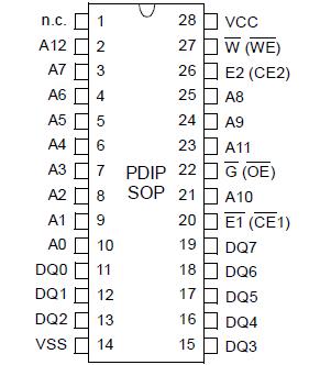
Features: ` 8192 x 8 bit static CMOS RAM
` 70 ns Access Times
` Common data inputs and outputs
` Three-state outputs
` Typ. operating supply current 70 ns: 10 mA
` Standby current:< 2 A at Ta 70 °C
` Data retention current at 2 V:< 1 A at Ta 70 °C
` TTL/CMOS-compatible
` Automatic reduction of power dissipation in long Read or Write cycles
` Power supply voltage 5 V
` Operating temperature ranges:
0 to 70 °C
-40 to 85 °C
-40 to 125 °C
` QS 9000 Quality Standard
` ESD protection > 2000 V
(MIL STD 883C M3015.7)
` Latch-up immunity > 100 mA
` Packages: PDIP28 (600 mil)
SOP28 (330 mil)
Pinout Specifications
| Absolute Maximum Ratings a |
Symbol |
Min. |
Max. |
Unit |
| Power Supply Voltage |
VCC |
-0.3 |
7 |
V |
| Input Voltage |
VI |
-0.3 |
VCC+0.5b |
V |
| Output Voltage |
VO |
-0.3 |
VCC+0.5b |
V |
| Power Dissipation |
PD |
- |
1 |
W |
Operating Temperature C-Type
K-Type
A-Type |
Ta |
0
-40
-40 |
70
85
125 |
|
Storage Temperature C/K-Type
A-Type |
Tstg |
|
125
150 |
|
Output Short-Circuit Current
at VCC = 5 V and VO = 0 V c |
| IOS | |
|
100 |
mA |
a Stresses greater than those listed under "Absolute Maximum Ratings" may cause permanent damage to the device. This is a stress rating only, and functional operation of the device at condition above those indicated in the operational sections of this specification is not implied.Exposure to absolute maximum rating conditions for extended periods may affect reliability
b Maximum voltage is 7 V
c Not more than 1 output should be shorted at the same time. Duration of the short circuit should not exceed 30 s.
DescriptionThe U6264B is a static RAM manufactured using a CMOS process technology with the following operating modes:
- Read - Standby
- Write - Data Retention
The memory array is based on a 6-transistor cell.
The U6264B is activated by the rising edge of E2 (at E1 = L), or the falling edge of E1 (at E2 = H). The address and control inputs open simultaneously. According to the information of W and G, the data inputs, or outputs, are active. In a Read cycle, the data outputs of U6264B are activated by the falling edge of G,afterwards the data word read will be available at the outputs DQ0 -DQ7. After the address change, the data outputs go High-Z until the new read information is available.
The data outputs of U6264B have no preferred state. If the memory is driven by CMOS levels in the active state, and if there is no change of the address, data input and control signals W or G, the operating current (at IO = 0 mA) drops to the value of the operating current in the Standby mode. The Read cycle of U6264B is finished by the falling edge of E2 or W, or by the rising edge of E1, respectively.
Data retention is guaranteed down to 2 V. With the exception of E2, all inputs consist of NOR gates, so that no pull-up/pull-down resistors are required. This gate circuit of U6264B allows to achieve low power standby requirements by activation
with TTL-levels too.If the circuit is inactivated by E2 = L, the standby current (TTL) drops to 150 A typ.

 U6264B Data Sheet


