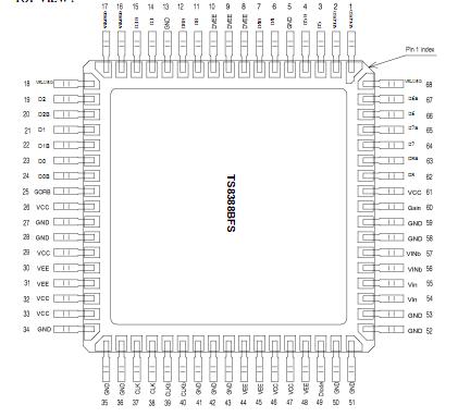
PinoutSpecifications Parameter Symbol Comments Values Unit Positive supply voltage VCC GND to 6 V Digital negative supply voltage DVEE GND to -5.7 V Digital positive supply voltage VPLUSD GND -0.3 to 2.8 V Negative s...
TSEV8388BFS: PinoutSpecifications Parameter Symbol Comments Values Unit Positive supply voltage VCC GND to 6 V Digital negative supply voltage DVEE GND to -...
SeekIC Buyer Protection PLUS - newly updated for 2013!
268 Transactions
All payment methods are secure and covered by SeekIC Buyer Protection PLUS.
Features: • 50Ω Input Clock and Data (Differential ECL) through 2.54 mm Pitch Connecto...
Specifications Parameter Symbol Comments Values Unit Positive supply volta...
Parameter |
Symbol |
Comments |
Values |
Unit |
Positive supply voltage |
VCC |
|
GND to 6 |
V |
Digital negative supply voltage |
DVEE |
|
GND to -5.7 |
V |
Digital positive supply voltage |
VPLUSD |
|
GND -0.3 to 2.8 |
V |
Negative supply voltage |
VEE |
|
VGND to -6 |
V |
Maximum difference between negative supply voltage |
DVEE to VEE |
|
0.3 |
V |
Analog input voltages |
VIN or VINB |
|
-1 to +1 |
V |
Maximum difference between VIN and VINB |
VIN - VINB |
|
-2 to +2 |
V |
Digital input voltage |
VD |
GORB |
-0.3 to VCC +0.3 |
V |
Digital input voltage |
VD |
DRRB |
VEE |
V |
Digital output voltage |
VO |
|
VPLUSD |
V |
Clock input voltage |
VCLK or VCLKB |
|
-3 to +1.5 |
V |
Maximum junction temperature |
VCLK - VCLKB |
|
-2 to +2 |
V |
Junction temperature |
TJ |
|
+145 |
°C |
Storage temperature |
Tstg |
|
- 65to + 150 |
°C |
Lead temperature (soldering 10s) |
Tleads |
|
+300 |
°C |
The TSEV8388BFS Evaluation Board (EB) is a prototype board which has been designed in order to facilitate the evaluation and the characterization of the TS8388BF device (in CQFP68) up to its 1.5 GHz full power bandwidth at up to 1 Gsps in the military temperature range.
The high speed of the TSEV8388BFS requires careful attention to circuit design and layout to achieve optimal performance. This four metal layer board with internal ground plane has the adequate functions in order to allow a quick and simple evaluation of the TS8388BF ADC performances over the temperature range.
The TSEV8388BFS Evaluation Board (EB) is very straightforward as it only implements the TS8388BF ADC device, SMA connectors for input / output accesses and a 2.54 mm pitch connector compatible with HP16500C high frequency probes.
The TSEV8388BFS also implements a de-embedding fixture in order to facilitate the evaluation of the high frequency insertion loss of the inputs microstrip lines, and a die junction temperature measurement setting.
The TSEV8388BFS is constituted by a sandwich of two dielectric layers, featuring low insertion loss and enhanced thermal characteristics for operation in the high frequency domain and extended temperature range.
The TSEV8388BFS dimensions are 130 mm x 130 mm.
The TSEV8388BFS set comes fully assembled and tested, with the TSX8388BF installed.