TSB12LV26-EP

Features: The TSB12LV26-EP device supports the following features:• Controlled Baseline• One Assembly/Test Site, One Fabrication Site• Extended Temperature Performance of 40°C to 110°C• Enhanced Diminishing Manufacturing Sources (DMS) Support• Enhanced Product Change ...

product image

TSB12LV26-EP Picture
SeekIC No. : 004529123 Detail

TSB12LV26-EP: Features: The TSB12LV26-EP device supports the following features:• Controlled Baseline• One Assembly/Test Site, One Fabrication Site• Extended Temperature Performance of 40°C to 1...

floor Price/Ceiling Price

Part Number:
TSB12LV26-EP
Supply Ability:
5000

Price Break

  • Qty
  • 1~5000
  • Unit Price
  • Negotiable
  • Processing time
  • 15 Days
Total Cost: $ 0.00

SeekIC Buyer Protection PLUS - newly updated for 2013!

  • Escrow Protection.
  • Guaranteed refunds.
  • Secure payments.
  • Learn more >>

Month Sales

268 Transactions

Rating

evaluate  (4.8 stars)

Upload time: 2025/1/11

Payment Methods

All payment methods are secure and covered by SeekIC Buyer Protection PLUS.

Notice: When you place an order, your payment is made to SeekIC and not to your seller. SeekIC only pays the seller after confirming you have received your order. We will also never share your payment details with your seller.
Product Details

Description


Features:

The TSB12LV26-EP device supports the following features:
• Controlled Baseline
• One Assembly/Test Site, One Fabrication Site
• Extended Temperature Performance of 40°C to 110°C
• Enhanced Diminishing Manufacturing Sources (DMS) Support
• Enhanced Product Change Notification
• Qualification Pedigree†
• 3.3-V and 5-V PCI bus signaling
• 3.3-V supply (core voltage is internally regulated to 1.8 V)
• Serial bus data rates of 100M bits/s, 200M bits/s, and 400M bits/s
• Physical write posting of up to three outstanding transactions
• Serial ROM interface supports 2-wire devices
• External cycle timer control for customized synchronization
• PCI burst transfers and deep FIFOs to tolerate large host latency
• Two general-purpose I/Os
• Fabricated in advanced low-power CMOS process
• Packaged in 100-terminal LQFP (PZ)
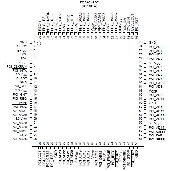
PCI_CLKRUN protocol


Pinout

  Connection Diagram


Specifications

Supply voltage range, VCC . . . . . . . . . . . . . . . . . . . . . . . . . . . . . . . . . . . .. . . . . . . . . . . . . . . . 0.5 V to 3.6 V
Supply voltage range, VCCP . . . . . . . . . . . . . . . . . . . . . . . . . . . . . . . . . . . .. . . . . . . . . . . . . . . 0.5 V to 5.5 V
Input voltage range for PCI, VI . . . . . . . . . . . . . . . . . . . . . . . . . . . . . . . . . .. . . . . . . . . . 0.5 to VCCP + 0.5 V
Input voltage range for miscellaneous and PHY interface, VI . . . . . . . . . . . . . . . . . . . . . 0.5 to VCCI + 0.5 V
Output voltage range for PCI, VO . . . . . . . . . . . . . . . . . . . . . . . . . . . . . . . . . . .  . . . . . . 0.5 to VCCP + 0.5 V
Input voltage range for miscellaneous and PHY interface, VO . . . . . . . . . . . . . . . . . . . . 0.5 to VCCP + 0.5 V
Input clamp current, IIK (VI < 0 or VI > VCC) (see Note 1) . . . . . . . . . . . . . . . . . . . .  . . . . . .  . . . . . . ±20 mA
Output clamp current, IOK (VO < 0 or VO > VCC) (see Note 2) . . . . . . . . . . . . . . . . . . . . . . . . . . . . . . ±20 mA
Operating free-air temperature range . . . . . . . . . . . . . . . . . . . . . . . . . . . . . . . . . . . . . . . . 40°C to 110°C
Storage temperature range . . . . . . . . . . . . . . . . . . . . . . . . . . . . . . . . . . . . . . . . . . . . . . . . 65°C to 150°C
† Stresses beyond those listed under absolute maximum ratings may cause permanent damage to the device. These are stress ratings only, and functional operation of the device at these or any other conditions beyond those indicated under recommended operating conditions is not implied. Exposure to absolute-maximum-rated conditions for extended periods may affect device reliability.
NOTES: 1. Applies to external input and bidirectional buffers. VI > VCCP.
2. Applies to external output and bidirectional buffers. VO > VCCP.


Description

The Texas Instruments TSB12LV26 device is a PCI-to-1394 host controller compliant with the PCI Local Bus Specification, PCI Bus Power Management Interface Specification, IEEE Std 1394-1995, and 1394 Open Host Controller Interface Specification. The chip provides the IEEE 1394 link function and is compatible with 100M bits/s, 200M bits/s, and 400M bits/s serial bus data rates.

As required by the 1394 Open Host Controller Interface Specification (OHCI) and IEEE Std 1394a-2000, internal control registers are memory-mapped and nonprefetchable. The PCI configuration header is accessed through configuration cycles specified by PCI and provides plug-and-play (PnP) compatibility. Furthermore, the TSB12LV26 device is compliant with the PCI Bus Power Management Interface Specification, per the PC 99 Design Guide requirements. TSB12LV26 device supports the D0, D2, and D3 power states.

The TSB12LV26 design provides PCI bus master bursting and is capable of transferring a cacheline of data at 132M bytes/s after connection to the memory controller. Since PCI latency can be large, deep FIFOs are provided to buffer 1394 data.

The TSB12LV26 device provides physical write posting buffers and a highly-tuned physical data path for SBP-2 performance. The TSB12LV26 device also provides multiple isochronous contexts, multiple cacheline burst transfers, advanced internal arbitration, and bus-holding buffers on the PHY/link interface.

An advanced CMOS process achieves low power consumption and allows the TSB12LV26 device to operate at PCI clock rates up to 33 MHz.


Customers Who Bought This Item Also Bought

Margin,quality,low-cost products with low minimum orders. Secure your online payments with SeekIC Buyer Protection.
Audio Products
Industrial Controls, Meters
Tapes, Adhesives
803
Isolators
View more