Features: ` Complete 1.4 GHz single-chip system
` Adaptive DC/DC converter driver output
` On-board tuning amplifier output
` Varicap drive disable
` Four NPN open-collector output ports (10 mA)
` Four bus-controlled bidirectional ports (NPN open-collector outputs)
` In-lock detector
` 5-step Analog-to-Digital Converter (ADC)
` Mixer/Oscillator (M/O) band-switch output
` 15-bit programmable divider
` Programmable reference divider ratio (512, 640 or 1024)
` Programmable charge-pump current (50 or 250 mA)
` I2C-bus format
Address plus four data bytes transmission (write mode)
Address plus one status byte transmission (read mode)
Four independent addresses
` Low power, low radiation.Application· Multimedia TV tuners and front-ends
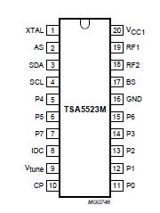
· VCR tuners.Pinout Specifications
| SYMBOL |
PARAMETER |
CONDITIONS |
MIN. |
MAX. |
UNIT |
| ViRF |
prescaler input voltage
|
|
-0.3 |
VCC1 |
V |
|
VCC1 |
supply voltage (+5 V) |
|
-0.3 |
+6 |
V |
| VoIDC |
IDC output voltage |
|
-0.3 |
VCC1 |
V |
| VoNPN |
NPN open-collector output voltage |
|
-0.3 |
+16 |
V |
| IoNPN |
NPN open-collector output current |
|
-1 |
+15 |
V |
| VoCP |
charge-pump output voltage |
|
-0.3 |
+Vcc1 |
V |
| Vo(tune) |
tuning voltage output |
see Fig.3 |
-0.3 |
+40 |
V |
| VoBS |
band-switch output voltage |
|
-0.3 |
Vcc1 |
V |
| ViSCL |
serial clock input voltage |
|
-0.3 |
+6 |
V |
| Vi/oSDA |
serial data input/output voltage |
|
-0.3 |
+6 |
V |
| IoSDA |
data output current |
|
-0.3 |
+5 |
V |
| ViAS |
address selection input voltage |
|
-0.3 |
+Vcc1 |
mA |
| ViXTAL |
crystal input voltage |
|
-0.3 |
+Vcc1 |
|
| Tstg |
IC storage temperature |
|
-40 |
+150 |
|
| tTj(max) |
maximum junction temperature |
|
- |
+150 |
s |
| tsc |
short-circuit time every pin to VCC1 or GND |
|
- |
10 |
s |
DescriptionThe TSA5523M is a single chip PLL frequency synthesizer designed for TV and VCR tuning systems. The circuit consists of a divide-by-eight prescaler with its own preamplifier, a 15-bit programmable divider, a crystal oscillator and its programmable reference divider, a phase/frequency detector combined with a charge-pump which drives the tuning amplifier, including 33 V output. Three NPN open-collector outputs are provided for band switching together with five open-collector NPN outputs. Four of these ports can also be used as input ports (one ADC and three general purpose I/O ports).
An output is provided to control a Philips mixer/oscillator IC controlled by bits P7, P5 and P4. Depending on the reference divider ratio (512, 640 or 1024), the phase comparator operates at 3.90625, 6.25 or 7.8125 kHz with a 4 MHz crystal.
The lock detector bit FL TSA5523M is set to logic 1 when the loop is locked and is read on the SDA line (status byte) during a read operation. The ADC is available for digital AFC control. The ADC code is read during a read operation on the I2C-bus. The ADC input is combined with the port P6. In the test mode, this port is also used as a test output for fref and fdiv/2 (see Table 4). In addition, the circuit includes a DC/DC converter driver connected to the IDC pin to control the amplitude of an external oscillator followed by a voltage rectifier.
The voltage rectifier TSA5523M is used to generate the correct tuning supply voltage to maintain a constant current into the tuning amplifier. The DC/DC converter driver can be disabled by setting the IDC pin to VCC1 in this event the tuning supply voltage is delivered by a fixed 33 V supply. Five serial bytes (including address byte) are required to address the device, select the VCO frequency, program the ports, set the charge-pump current and set the reference divider ratio. The device has four independent I2C-bus addresses which can be selected by applying a specific voltage on the AS input (see Table 3).

 TSA5523M Data Sheet


