Features: ` Complete 1.3 GHz single chip system` Four PNP band switch buffers (40 mA)` 33 V output tuning voltage` In-lock detector` 15-bit programmable divider` Programmable reference divider ratio (512, 640 or 1024)` Programmable charge-pump current (60 or 280 mA)` Varicap drive disable` Univers...
TSA5520: Features: ` Complete 1.3 GHz single chip system` Four PNP band switch buffers (40 mA)` 33 V output tuning voltage` In-lock detector` 15-bit programmable divider` Programmable reference divider ratio...
SeekIC Buyer Protection PLUS - newly updated for 2013!
268 Transactions
All payment methods are secure and covered by SeekIC Buyer Protection PLUS.
` Complete 1.3 GHz single chip system
` Four PNP band switch buffers (40 mA)
` 33 V output tuning voltage
` In-lock detector
` 15-bit programmable divider
` Programmable reference divider ratio (512, 640 or 1024)
` Programmable charge-pump current (60 or 280 mA)
` Varicap drive disable
` Universal bus protocol I2C-bus or 3-wire bus (the TSA5520/TSA5521 I2C-bus mode only includes the write mode; if both read and write modes are required the TSA5526/TSA5527 devices should be selected):
bus protocol for 18 or 19 bits transmission (3-wire bus)
extra protocol for 27 bits for test and features (3-wire bus)
address plus 4 data bytes transmission (I2C-bus)
three independent I2C-bus addresses
` Low power and low radiation.
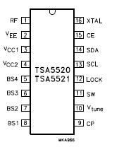
SYMBOL | PARAMETER | MIN. | MAX. | UNIT |
VCC1 | supply voltage; +5 V (pin 3) |
-0.3 | +6.0 | V |
VCC2 |
band switch supply voltage; +12 V (pin 4) | -0.3 | +16 | V |
Vi(RF) | prescaler input voltage (pin 1) | -0.3 | +Vcc1 | V |
Vo(BSn) | band switch buffers output voltage (pins 5 to 8) | -0.3 | +Vcc2 | V |
Io(BSn) | band switch buffers output current | -1 | +50 | mA |
Vo(CP) | charge-pump output voltage (pin 9) | -0.3 | +Vcc1 | V |
Vo(tune) | output tuning voltage (pin 10) | -0.3 | +35 | V |
Vi(SW) | input switching voltage (pin 11) | -0.3 | Vcc1 | V |
Vo(LOCK) | lock output voltage (pin 12) | -0.3 | +Vcc1 | V |
Vi(SCL) | serial clock input voltage (pin 13) | -0.3 | +6.0 | V |
Vi/o(SDA) | serial data input/output voltage (pin 14) | -0.3 | +6.0 | V |
Io(SDA) | serial data output current | -0.3 | +10 | mA |
Vi(CE) | chip enable input voltage (pin 15) | -0.3 | +6.0 | V |
Vi(xtal) | crystal oscillator input voltage (pin 16) | -0.3 | +Vcc1 | V |
Tstg | storage temperature | -40 | +150 | |
Tj | maximum junction temperature | - | +150 | |
tsc | short-circuit time; every pin except pin 4 to pin 3 and every pin to pin 2; note 1 | - | 10 | s |
The TSA5520 is a single-chip PLL frequency synthesizer designed for TV and VCR tuning systems. The circuit
consists of a divide-by-eight prescaler with its own preamplifier, a 15-bit programmable divider, a crystal
oscillator and its programmable reference divider and a phase/frequency detector combined with a charge-pump
which drives the tuning amplifier and the 33 V output. Four high-current PNP band switch buffers are provided
for band switching. Two PNP buffers can be switched on simultaneously. The sum of the collector currents is limited
to 50 mA.