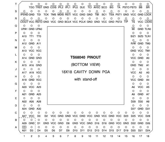
Features: 26-42 MIPS Integer Performance3.5-5.6 MFLOPS Floating-Point-PerformanceIEEE 754-Compatible FPUIndependent Instruction and Data MMUs4K bytes Physical Instruction Cache and 4K bytes Physical Data Cache Accessed Simultaneously32-bit, Nonmultiplexed External Address and Data Buses with Synch...
TS68040: Features: 26-42 MIPS Integer Performance3.5-5.6 MFLOPS Floating-Point-PerformanceIEEE 754-Compatible FPUIndependent Instruction and Data MMUs4K bytes Physical Instruction Cache and 4K bytes Physical...
SeekIC Buyer Protection PLUS - newly updated for 2013!
268 Transactions
All payment methods are secure and covered by SeekIC Buyer Protection PLUS.
Symbol |
Parameter |
Condition |
Min |
Max |
Unit |
VCC | Supply Voltage Range | -0.3 |
7.0 | V | |
VI | Input Voltage Range | -0.3 | 7.0 | V | |
PD | Power Dissipation | Large buffers enabled | 7.7 | W | |
Small buffers enabled | 6.3 | W | |||
TC | Operating Temperature | -55 | TJ | °C | |
Tstg | Storage Temperature Range | -65 | +150 | °C | |
TJ | Junction Temperature(1) | +120 | °C | ||
Tlead | Lead Temperature | Max.10 sec soldering | +300 | °C |
The TS68040 is Atmel's third generation of 68000-compatible, high-performance, 32-bit microprocessors. The TS68040 is a virtual memory microprocessor employing multiple, concurrent execution units and a highly integrated architecture to provide very high performance in a monolithic HCMOS device. On a single chip, the TS68040 integrates a 68030-compatible integer unit, an IEEE 754-compatible floating-point unit (FPU), and fully independent instruction and data demand-paged memory manage- ment units (MMUs), including 4K bytes independent instruction and data caches. Ahigh degree of instruction execution parallelism is achieved through the use of multi-ple independent execution pipelines, multiple internal buses, and a full internal Harvard architecture, including separate physical caches for both instruction and data accesses. The TS68040 also directly supports cache coherency in multimaster appli-cations with dedicated on-chip bus snooping logic.
The TS68040 is user-object-code compatible with previous members of the TS68000 Family and is specifically optimized to reduce the execution time of compiler-gener- ated code. The 68040 HCMOS technology, provides an ideal balance between speed,power, and physical device size.
Figure 1 is a simplified block diagram of the TS68040. Instruction execution is pipe-lined in both the integer unit and FPU. Independent data and instruction MMUs control the main caches and the address translation caches (ATCs). The ATCs speed up log-ical-to-physical address translations by storing recently used translations. The bussnooper circuit ensures cache coherency in multimaster and multiprocessing applications.