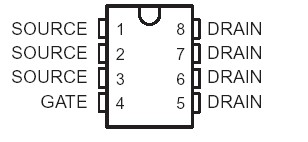
Features: Low rDS(on) . . . 0.18 at VGS = 10 V3-V CompatibleRequires No External VCCTTL and CMOS Compatible InputsVGS(th) = 1.5 V MaxESD Protection Up to 2 kV per MIL-STD-883C, Method 3015PinoutSpecifications UNIT Drain-to-source voltage, VDS 15 V Gate-to-source voltage, VGS ...
TPS1100: Features: Low rDS(on) . . . 0.18 at VGS = 10 V3-V CompatibleRequires No External VCCTTL and CMOS Compatible InputsVGS(th) = 1.5 V MaxESD Protection Up to 2 kV per MIL-STD-883C, Method 3015PinoutSpe...
SeekIC Buyer Protection PLUS - newly updated for 2013!
268 Transactions
All payment methods are secure and covered by SeekIC Buyer Protection PLUS.
UNIT | |||||
Drain-to-source voltage, VDS |
15 |
V | |||
Gate-to-source voltage, VGS |
2 or 15 |
V | |||
Continuous drain current (TJ = 150°C) ID‡ |
VGS = 2.7 V | D package |
TA = 25°C |
±0.41 |
A |
TA= 125°C |
±0.28 | ||||
PW package |
TA = 25°C |
±0.4 | |||
TA = 125°C |
±0.23 | ||||
VGS = 3 V | D package |
TA = 25°C |
±0.6 | ||
TA = 125°C |
±033 | ||||
PW package |
TA = 25°C |
±0.33 | |||
TA = 125°C |
±0.27 | ||||
VGS = 4.5 V | D package |
TA = 25°C |
±1 | ||
TA = 125°C |
±047 | ||||
PW package |
TA = 25°C |
±0.81 | |||
TA = 125°C |
±0.37 | ||||
VGS = 10 V | D package |
TA = 25°C |
±1.6 | ||
TA = 125°C |
±0.72 | ||||
PW package |
TA = 25°C |
1.27 | |||
TA= 125°C |
±58 | ||||
Pulsed drain current, ID‡ |
TA = 25°C |
±7 |
A | ||
Continuous source current (diode conduction), IS |
TA = 25°C |
1 |
A | ||
Storage temperature range, Tstg |
55 to 150 |
°C | |||
Operating junction temperature range, TJ |
40 to 150 |
°C | |||
Operating free-air temperature range, TA |
40 to 125 |
°C | |||
Lead temperature 1,6 mm (1/16 inch) from case for 10 seconds |
260 |
°C |
The TPS1100 is a single P-channel enhancement-mode MOSFET. The device has been optimized for 3-V or 5-V power distribution in battery-powered systems by means of Texas Instruments LinBiCMOSE process. With a maximum VGS(th) of 1.5 V and an IDSS of only 0.5 A, the TPS1100 is the ideal high-side switch for low-voltage, portable battery-management systems where maximizing battery life is a primary concern. The low rDS(on) and excellent ac characteristics (rise time 10 ns typical) make the TPS1100 the logical choice for low-voltage switching applications such as power switches for pulse-width-modulated (PWM) controllers or motor/bridge drivers.
The ultrathin thin shrink small-outline package or TSSOP (PW) version with its smaller footprint and reduction in height fits in places where other P-channel MOSFETs cannot. The size advantage of TPS1100 is especially important where board real estate is at a premium and height restrictions do not allow for a small-outline integrated circuit (SOIC) package.