TMS470R1VC3482

Features: ` High-Performance Static CMOS Technology` TMS470R1x 16/32-Bit RISC Core (ARM7TDMI™) 24-MHz System Clock (48-MHz Pipeline Mode) Independent 16/32-Bit Instruction Set Open Architecture With Third-Party Support Built-In Debug Module Utilizes Big-Endian Format` Integrated Memory 25...

product image

TMS470R1VC3482 Picture
SeekIC No. : 004525149 Detail

TMS470R1VC3482: Features: ` High-Performance Static CMOS Technology` TMS470R1x 16/32-Bit RISC Core (ARM7TDMI™) 24-MHz System Clock (48-MHz Pipeline Mode) Independent 16/32-Bit Instruction Set Open Architect...

floor Price/Ceiling Price

Part Number:
TMS470R1VC3482
Supply Ability:
5000

Price Break

  • Qty
  • 1~5000
  • Unit Price
  • Negotiable
  • Processing time
  • 15 Days
Total Cost: $ 0.00

SeekIC Buyer Protection PLUS - newly updated for 2013!

  • Escrow Protection.
  • Guaranteed refunds.
  • Secure payments.
  • Learn more >>

Month Sales

268 Transactions

Rating

evaluate  (4.8 stars)

Upload time: 2025/1/11

Payment Methods

All payment methods are secure and covered by SeekIC Buyer Protection PLUS.

Notice: When you place an order, your payment is made to SeekIC and not to your seller. SeekIC only pays the seller after confirming you have received your order. We will also never share your payment details with your seller.
Product Details

Description


Features:

` High-Performance Static CMOS Technology
` TMS470R1x 16/32-Bit RISC Core (ARM7TDMI™)
24-MHz System Clock (48-MHz Pipeline Mode)
Independent 16/32-Bit Instruction Set
Open Architecture With Third-Party Support
Built-In Debug Module
Utilizes Big-Endian Format
` Integrated Memory
256K-Byte Program ROM
ROM Pipeline Wrapper (RPW)
10K-Byte Static RAM (SRAM) (VC3x8)
12K-Byte Static RAM (SRAM) (VC3x82)
` Operating Features
Core Supply Voltage (VCC): 1.81 V - 2.06 V
Core Supply Voltage (VCC): 1.70 V - 2.06 V
  When Used from −40 to 85C
I/O Supply Voltage (VCCIO): 3.0 V - 3.6 V
Low-Power Modes: STANDBY and HALT
Industrial and Automotive Temperature Ranges
` 470+ System Module
32-Bit Address Space Decoding
Bus Supervision for Memory and Peripherals
Analog Watchdog (AWD) Timer
Real-Time Interrupt (RTI)
System Integrity and Failure Detection
` Zero-Pin Phase-Locked Loop (ZPLL)-Based
  Clock Module With Prescaler
Multiply-by-4 or -8 Internal ZPLL Option
ZPLL Bypass Mode
` Six Communication Interfaces:
Two Serial Peripheral Interfaces (SPIs)
255 Programmable Baud Rates
Two Serial Communications Interfaces (SCIs)
224 Selectable Baud Rates
Asynchronous/Isosynchronous Modes
Standard CAN Controller (SCC)
16-Mailbox Capacity
Fully Compliant With CAN Protocol, Version 2.0B
Class II Serial Interface (C2SIb)
Two Selectable Data Rates
Normal Mode 10.4 Kbps and 4X Mode 41.6 Kbps
` High-End Timer (HET)
27 Programmable I/O Channels (VC338x):
23 High-Resolution Pins
4 Standard-Resolution Pins
16 Programmable I/O Channels (VC348x):
14 High-Resolution Pins
2 Standard-Resolution Pins
High-Resolution Share Feature (XOR)
High-End Timer RAM
64-Instruction Capacity
` 10-Bit Multi-Buffered ADC (MibADC)
  12-Channel (VC338x)
  16-Channel (VC348x)
64-Word FIFO Buffer
Single- or Continuous-Conversion Modes
1.55 s Minimum Sample and Conversion Time
Calibration Mode and Self-Test Features
` Eight External Interrupts
` Flexible Interrupt Handling
` 5 Dedicated General-Purpose I/O (GIO) Pins,
  1 Input-Only GIO Pin, and 48 Additional
  Peripheral I/Os (VC338x)
` 11 Dedicated GIO Pins,1 Input-Only GIO Pin,
  and 38 Additional Peripheral I/Os (VC348x)
` External Clock Prescale (ECP) Module
Programmable Low-Frequency External Clock (CLK)
` Compatible ROM Device
` On-Chip Scan-Base Emulation Logic,
  IEEE Standard 1149.1† (JTAG) Test-Access Port
` 100-Pin Plastic Low-Profile Quad Flatpack (PZ Suffix)
` Development System Support Tools Available
Code Composer Studio™ Integrated
  Development Environment (IDE)
HET Assembler and Simulator
Real-Time In-Circuit Emulation


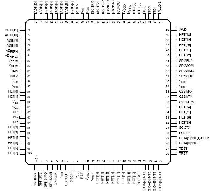
Pinout

  Connection Diagram


Specifications

Supply voltage ranges: VCC, VCCF (see Note 1) . . . . . . . . . . . . . . . . . . . . . . . . . . . . . . . . . . . . . . −0.3 V to 2.5 V
Supply voltage ranges: VCCIO, VCCAD (see Note 1) . . . . . . . . . . . . . . . . . . . . . . . . . . . . . . . . . . . .−0.3 V to 4.1V
Input voltage range: All input pins . . . . . . . . . . . . . . . . . . . . . . . . . . . . . . . . . . . . . . . . . . . . . . . . . −0.3 V to 4.1 V
Input clamp current: IIK (VI < 0 or VI > VCCIO)
All pins except ADIN[0:11]‡, PORRST, TRST, TEST and TCK . . . . . . . . . . . . . . . . . . . . . . . . . . . . . . . . . . . .− ±20 mA
IIK (VI < 0 or VI > VCCAD)
ADIN[0:11]‡ . . . . . . . . . . . . . . . . . . . . . . . . . . . . . . . . . . . . . . . . . . . . . . . . . . . . . . . . . . . . . . . . . . . . . . . − ±10 mA
Operating free-air temperature ranges, TA: A version (VC348x). . . . . . . . . . . . . . . . . . . . . . . . . . .   −40°C to 85°C
T version (VC348x). . . . . . . . . . . . . . . . . . . . . . . . . . . . . . . . . . . . . . . . . . . . . . . . . . . . . . . . . . . . .  −40°C to 105°C
Q version (VC338x) . . . . . . . . . . . . . . . . . . . . . . . . . . . . . . . . . . . . . . . . . . . . . . . . . . . . . . . . . . . .−−40°C to 125°C
Operating junction temperature range, TJ . . . . . . . . . . . . . . . . . . . . . . . . . . . . . . . . . . . . . . . . . . . .−40°C to 150°C
Storage temperature range, Tstg . . . . . . . . . . . . . . . . . . . . . . . . . . . . . . . . . . . . . . . . . . . . . . . . . . −65°C to 150°C
† Stresses beyond those listed under "absolute maximum ratings" may cause permanent damage to the device. These are stress ratings only,
and functional operation of the device at these or any other conditions beyond those indicated under "recommended operating conditions" is
not implied. Exposure to absolute-maximum-rated conditions for extended periods may affect device reliability.
‡ ADIN[0:11] for VC338x only and ADIN[0:15] for VC348x only.
NOTE 1: All voltage values are with respect to their associated grounds.


Description

The TMS470R1VC338, TMS470R1VC348, TMS470R1VC3382, and TMS470R1VC3482† devices are members of the Texas Instruments TMS470R1x family of general-purpose16/32-bit reduced instruction set computer (RISC) microcontrollers. The VC3x8x microcontroller offers high performance utilizing the high-speed ARM7TDMI 16/32-bit RISC central processing unit (CPU), resulting in a high instruction throughput while maintaining greater code efficiency. The ARM7TDMI 16/32-bit RISC CPU views memory as a linear collection of bytes numbered upwards from zero. The TMS470R1VC3x8x utilizes the big-endian format where the most significant byte of a word is stored at the lowest numbered byte and the least significant byte at the highest numbered byte.

High-end embedded control applications demand more performance from their controllers while maintaining low costs. The VC3x8x RISC core architecture offers solutions to these performance and cost demands while maintaining low power consumption.

The VC338/VC348/VC3382/VC3482 device contains the following:
· ARM7TDMI 16/32-Bit RISC CPU
· TMS470R1x system module (SYS) with 470+ enhancements
· 256K-byte ROM
· 10K-byte SRAM (VC3x8)
· 12K-byte SRAM (VC3x82)
· Zero-pin phase-locked loop (ZPLL) clock module
· Analog watchdog (AWD) timer
· Real-time interrupt (RTI) module
· Two serial peripheral interface (SPI) modules
· Two serial communications interface (SCI) modules
· Standard CAN controller (SCC)
· Class II serial interface (C2SIb)
· 10-bit multi-buffered analog-to-digital converter (MibADC), 12-input channels (VC338x), 16-input channels (VC348x)
· High-end timer (HET) controlling 27 I/Os (VC338x), controlling 16 I/Os (VC348x)
· External Clock Prescale (ECP)
· Up to 53 I/O pins and 1 input-only pin (VC338x), up to 49 I/O pins and 1 input-only pin (VC348x)

The functions performed by the 470+ system module (SYS) include: address decoding; memory protection; memory and peripherals bus supervision; reset and abort exception management; prioritization for all internal interrupt sources; device clock control; and parallel signature analysis (PSA). This data sheet includes devicespecific information such as memory and peripheral select assignment, interrupt priority, and a device memory map. For a more detailed functional description of the SYS module, see the TMS470R1x System Module Reference Guide (literature number SPNU189).

The VC3x8x memory includes general-purpose SRAM supporting single-cycle read/write accesses in byte, half-word, and word modes.

The ROM memory on this device is programmable read-only memory that is masked at the time of device fabrication. The ROM operates with a system clock frequency of up to 24 MHz. In pipeline mode, the ROM operates with a system clock frequency of up to 48MHz. For more detailed information on the ROM Pipeline Wrapper, see the TMS470R1x ROM Pipeline Wrapper (RPW) Reference Guide (literature number SPNU009).


Customers Who Bought This Item Also Bought

Margin,quality,low-cost products with low minimum orders. Secure your online payments with SeekIC Buyer Protection.
Soldering, Desoldering, Rework Products
Cable Assemblies
Cables, Wires - Management
Programmers, Development Systems
Semiconductor Modules
Industrial Controls, Meters
View more