TMS470R1A288

Features: ` High-Performance Static CMOS Technology ` Fully Compliant With CAN Protocol,` TMS470R1x 16/32-Bit RISC Core Version 2.0B (ARM7TDMI™) Three Inter-Integrated Circuit (I2C) Modules 24-MHz System Clock (48-MHz Pipeline) ` Multi-Master and Slave Interfaces Independent 16/32-Bit Inst...

product image

TMS470R1A288 Picture
SeekIC No. : 004525143 Detail

TMS470R1A288: Features: ` High-Performance Static CMOS Technology ` Fully Compliant With CAN Protocol,` TMS470R1x 16/32-Bit RISC Core Version 2.0B (ARM7TDMI™) Three Inter-Integrated Circuit (I2C) Modules 2...

floor Price/Ceiling Price

Part Number:
TMS470R1A288
Supply Ability:
5000

Price Break

  • Qty
  • 1~5000
  • Unit Price
  • Negotiable
  • Processing time
  • 15 Days
Total Cost: $ 0.00

SeekIC Buyer Protection PLUS - newly updated for 2013!

  • Escrow Protection.
  • Guaranteed refunds.
  • Secure payments.
  • Learn more >>

Month Sales

268 Transactions

Rating

evaluate  (4.8 stars)

Upload time: 2025/1/11

Payment Methods

All payment methods are secure and covered by SeekIC Buyer Protection PLUS.

Notice: When you place an order, your payment is made to SeekIC and not to your seller. SeekIC only pays the seller after confirming you have received your order. We will also never share your payment details with your seller.
Product Details

Description


Features:

` High-Performance Static CMOS Technology
` Fully Compliant With CAN Protocol,
` TMS470R1x 16/32-Bit RISC Core Version 2.0B (ARM7TDMI™)
     Three Inter-Integrated Circuit (I2C) Modules
    24-MHz System Clock (48-MHz Pipeline)
` Multi-Master and Slave Interfaces
    Independent 16/32-Bit Instruction Set
` Up to 400 Kbps (Fast Mode)
    Open Architecture With Third-Party Support
` 7- and 10-Bit Address Capability
    Built-In Debug Module
` High-End Timer Lite (HET)
` Integrated Memory 12 Programmable I/O Channels:
    288K-Byte Program Flash
` 12 High-Resolution Pins
` Two Banks With 8 Contiguous Sectors High-Resolution Share Feature (XOR)
    16K-Byte Static RAM (SRAM) High-End Timer RAM
    Memory Security Module (MSM)
` 64-Instruction Capacity
    JTAG Security Module
` External Clock Prescale (ECP) Module
` Operating Features
    Programmable Low-Frequency External
    Low-Power Modes: STANDBY and HALT Clock (CLK)
    Industrial Temperature Range
` 12-Channel 10-Bit Multi-Buffered ADC
` 470+ System Module (MibADC)
    32-Bit Address Space Decoding
    64-Word FIFO Buffer
    Bus Supervision for Memory/Peripherals
    Single- or Continuous-Conversion Modes
    Digital Watchdog (DWD) Timer
    1.55 s Minimum Sample/Conversion Time
    Analog Watchdog (AWD) Timer
    Calibration Mode and Self-Test Features
    Enhanced Real-Time Interrupt (RTI)
` Flexible Interrupt Handling
    Interrupt Expansion Module (IEM)
` Expansion Bus Module (EBM) (PGE only)
    System Integrity and Failure Detection
    Supports 8- and 16-Bit Expansion Bus Memory Interface Mappings
    ICE Breaker
    42 I/O Expansion Bus Pins
` Direct Memory Access (DMA) Controller
` 50 Dedicated General-Purpose I/O (GIO) Pins
    32 Control Packets and 16 Channels and 43 Additional Peripheral I/Os (PGE)
` Zero-Pin Phase-Locked Loop (ZPLL)-Based
` 14 Dedicated General-Purpose I/O (GIO) Pins
    Clock Module With Prescaler and 43 Additional Peripheral I/Os (PZ)
    Multiply-by-8 Internal ZPLL Option
` 16 External Interrupts
    ZPLL Bypass Mode
` On-Chip Scan-Base Emulation Logic, IEEE
` Ten Communication Interfaces: Standard 1149.1(1) (JTAG) Test-Access Port
    Two Serial Peripheral Interfaces (SPIs)
` 144-Pin Plastic Low-Profile Quad Flatpack
` 255 Programmable Baud Rates (PGE Suffix)
    Two Serial Communication Interfaces (SCIs)
` 100-Pin Plastic Low-Profile Quad Flatpack (PZ
` 224 Selectable Baud Rates Suffix)
` Asynchronous/Isosynchronous Modes (1) The test-access port is compatible with the IEEE Standard
    1149.1-1990, IEEE Standard Test-Access Port and Boundary
    Class II Serial Interface B (C2SIb) Scan Architecture specification. Boundary scan is not
` Normal 10.4 Kbps and 4X Mode 41.6 Kbps supported on this device.
    Two Standard CAN Controllers (SCC)


Pinout

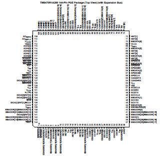
  Connection Diagram


Specifications

over operating free-air temperature range, A version unless otherwise noted(1)
Supply voltage range: VCC(2)............................................................................ -0.3 V to 2.5 V
Supply voltage range: VCCIO , VCCAD , VCCP (flash pump)(2) ............................-0.3 V to 4.1V
Input voltage range: All 5 V- tolerant input pins.................................................. -0.3 V to 6.0V
All other input pins ...............................................................................................-0.3 V to 4.1V
Input clamp current: All 5-V tolerant pins, PORRST, TRST, TEST, and TCK (VI <0) .......-20 mA(3)
ADIN[0:11] IIK (VI < 0 or VI > VCCAD) ..........................................................................±10 mA
All other pins IIK (VI < 0 or VI > VCCAD)....................................................................... ±20 mA
Operating free-air tempera- A version.................................................................. -40  to 85
ture ranges, TA
Operating junction tempera- ................................................................................-40 to 150
ture range, TJ
Storage temperature range, Tstg ........................................................................-40  to 150

(1) Stresses beyond those listed under "Absolute Maximum Ratings" may cause permanent damage to the device. These are stress ratings only, and functional operation of the device at these or any other conditions beyond those indicated under "Recommended Operating Conditions" is not implied. Exposure to absolute-maximum-rated conditions for extended periods may affect device reliability.
(2) All voltage values are with respect to their associated grounds.
(3) These pins do not have an internal clamp diode to a positive supply voltage.


Description

TMS470R1A288 16/32-bit reduced instruction set computer (RISC) microcontrollers. The A288 microcontroller offers high performance utilizing the high-speed ARM7TDMI 16/32-bit RISC central processing unit (CPU), resulting in a high instruction throughput while maintaining greater code efficiency. The ARM7TDMI 16/32-bit RISC CPU views memory as a linear collection of bytes numbered upwards from zero. The A288 utilizes the big-endian format where the most significant byte of a word is stored at the lowest-numbered byte and the least significant byte at the highest numbered byte.

High-end embedded control applications demand more performance from their controllers while maintaining low
costs. The A288 RISC core architecture offers solutions to these performance and cost demands while maintaining low power consumption.

The A288 devices contain the following:
· ARM7TDMI 16/32-Bit RISC CPU
· TMS470R1x system module (SYS) with 470+ enhancements
· 288K-byte flash
· 16K-byte SRAM
· Zero-pin phase-locked loop (ZPLL) clock module
· Digital watchdog (DWD) timer
· Analog watchdog (AWD) timer
· Enhanced real-time interrupt (RTI) module
· Interrupt expansion module (IEM)
· Memory security module (MSM)
· JTAG security module (JSM)
· Two serial peripheral interface (SPI) modules
· Two serial communications interface (SCI) modules
· Two standard CAN controllers (SCC)
· Three inter-integrated circuit (I2C) modules
· Class II serial interface B (C2SIb) module
· 10-bit multi-buffered analog-to-digital converter (MibADC), with 12 input channels
· High-end timer lite (HET) controlling 12 I/Os
· External clock prescale (ECP)
· Expansion bus module (EBM)
· Up to 93 I/O pins (PGE only), up to 57 I/O (PZ only)
The functions performed by the 470+ system module (SYS) include:
· Address decoding
· Memory protection
· Memory and peripherals bus supervision
· Reset and abort exception management
· Prioritization for all internal interrupt sources
· Device clock control
· Parallel signature analysis (PSA)

The enhanced real-time interrupt (RTI) module on the A288 has the option to be driven by the oscillator clock. The digital watchdog (DWD) is a 25-bit resettable decrementing counter that provides a system reset when the watchdog counter expires. This data sheet includes device-specific information such as memory and peripheral select assignment, interrupt priority, and a device memory map. For a more detailed functional description of the SYS module, see the TMS470R1x System Module Reference Guide (literature number SPNU189).

The A288 memory includes general-purpose SRAM supporting single-cycle read/write accesses in byte, half-word, and word modes.


Customers Who Bought This Item Also Bought

Margin,quality,low-cost products with low minimum orders. Secure your online payments with SeekIC Buyer Protection.
Prototyping Products
DE1
LED Products
Connectors, Interconnects
Audio Products
View more