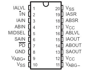
Pinout Specifications
Positive supply voltage, VCC (see Note 1) . . . . . . . . . . . . . . . . . . . . . . . . . . . . . . . 4.4 V
Negative supply voltage, VSS (see Note 2) . . . . . . . . . . . . . . . . . . . . . . . . . . . . . 11.1 V
Positive ABG supply voltage, VABG + . . . . . . . . . . . . . . . . . . . . . . . . . . . .. . . . . . . .5.6 V
Negative ABG supply voltage, VABG . . . . . . . . . . . . . . . . . . . . . . . . . . . . . . . . . . . . 8 V
ABG supply voltage differential (VABG+ VSS) . . . . . . . . . . . . . . . . . . . . . . . . . . . .15.2 V
Continuous total power dissipation at (or below), TA 25°C:
Unmounted device (see Figure 3). . . . . . . . . . . . . . . . . . . . . . . . . . . . .. . . .. . . . 825 mW
Mounted device (see Figure 3) . . . . . . . . . . . . . . . . . . . . . . . . . . . . . . . .. . . . . 1150 mW
Operating free-air temperature range, TA. . . . . . . . . . . . . . . . . . . . .. . . . 20°C to 45°C
Storage temperature range, TSTG. . . . . . . . . . . . . . . . . . . . . . . . . . . . . 55°C to 125°C
Lead temperature 1,6 mm (1/16 inch) from case for 10 seconds. . . . . . . . . . . . . 260°C
DescriptionThe TMS3473B is a monolithic CMOS integrated circuit designed to drive the parallel image-area gate (IAG), parallel storage-area gate (SAG), and antiblooming gate (ABG) inputs of the Texas Instruments (TI™) virtual-phase CCD image sensors. The TMS3473B interfaces the CCD image sensor to a user-defined timing generator; it receives TTL-input signals from the timing generator and outputs level-shifted and slew-rate-adjusted signals to the image sensor.
The TMS3473B allows operation of the CCD image sensor in either the interlace or noninterlace mode. When the TMS3473BI/N input is connected to VSS, the interlace mode is selected (see Figure 1); when I/N is connected to VCC, the noninterlace mode is selected (see Figure 2).
ABOUT follows ABIN and switches between VABG+ and VABG. IAOUT and SAOUT follow IAIN and SAIN, respectively, and switch between VCC and VSS. Additionally, ABOUT and IAOUT can each be made to output midlevel voltages. DC inputs to ABLVL and IALVL determine the midlevel voltages that can be output on ABOUT and IAOUT, respectively. A high-logic level on MIDSEL causes ABOUT to output its midlevel voltage; a low-logic level on MIDSEL causes IAOUT to output its midlevel voltage if the interlace mode is selected.Slew-rate adjustment of IAOUT and ABOUT is accomplished by connecting IASR to VCC and ABSR to VABG+ through external resistors. The larger the resistor values, the longer the rise and fall times are.A low-logic level on PD causes the TMS3473B to power down and all outputs to assume their low levels (IAOUT and SAOUT to VSS, ABOUT to VABG).
The TMS3473B is supplied in a 20-pin surface-mount package (DW) and is characterized for operation from 20°C to 45°C.

 TMS3473B Data Sheet


