Features: • TTL-Compatible Inputs
• CCD-Compatible Outputs
• Variable-Output Slew Rates With External Resistor Control
• Frame-Transfer Operation
• Solid-State Reliability
• Adjustable Clock LevelsPinout Specifications
Positive supply voltage, VCC (see Note 1) . . . . . . . . . . . . . . . . . . . . . . . . . . . . . . . . . . . . . . . . . . . . . . . . . . . . . . 3 V
Negative supply voltage, VSS (see Note 2) . . . . . . . . . . . . . . . . . . . . . . . . . . . . . . . . . . . . . . . . . . . . . . . . . 11.1 V
Continuous total power dissipation at (or below), TA 3 25°C:
Unmounted device (see Figure 1) . . . . . . . . . . . . . . 825 mW
Mounted device (see Figure 1) . . . . . . . . . . . . . . . . 1150 mW
Operating free-air temperature range, TA . . . . . . . . . . . . . . . . . . . . . . . . . . . . . . . . . . . . . . . . . . . 20°C to 45°C
Storage temperature range, TSTG . . . . . . . . . . . . . . . . . . . . . . . . . . . . . . . . . . . . . . . . . . . . . . . . . 55°C to 125°C
Lead temperature 1,6 mm (1/16 inch) from case for 10 seconds . . . . . . . . . . . . . . . . . . . . . . . . . . . . . . . 260°C
† Stresses beyond those listed under "absolute maximum ratings" may cause permanent damage to the device. These are stress ratings only, and functional operation of the device at these or any other conditions beyond those indicated under "recommended operating conditions" is not implied. Exposure to absolute-maximum-rated conditions for extended periods may affect device reliability.
NOTES:
1. All voltage values are with respect to GND.
2. The algebraic convention, in which the least positive (most negative) value is designated minimum, is used in this data sheet for voltage levels only.
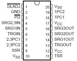
DescriptionThe TMS3472A serial driver is a monolithic CMOS integrated circuit designed to drive the serial-register gate (SRGn) and transfer-gate (TRG) inputs of the Texas Instruments (TIE) TC241 (monochrome) CCD image sensor. The TMS3472A interfaces the TI TMS3471C or a user-defined timing generator to the TC241; it receives TTL signals from the timing generator and outputs level-shifted and slew-rate-adjusted signals to the image sensor. The TMS3472A contains three noninverting serial drivers and one noninverting transfer driver as well as circuitry for slew-rate adjustment.
The voltage levels on SRG1OUT, SRG2OUT, SRG3OUT, and TRGOUT are controlled by the levels on VSS and VCC. DLADJ, PD, SRG1IN, SRG2,3IN, and TRGIN are TTL compatible. A high level on PD allows the TMS3472 to operate normally with the level-shifted and slew-rate-adjusted outputs following the inputs. When PD is low, the device is in a low power-consumption mode and all outputs are at VCC.The slew rate of SRG1OUT, SRG2OUT, and SRG3OUT is controlled by connecting a resistor between VCC and SSR. The TRGOUT slew rate is controlled by connecting a resistor between VCC and TSR. The larger the resistor values, the longer the rise and fall times are.The TMS3472A is available in a 20-pin surface-mount package (DW) and is characterized for operation from 20°C to 45°C.

 TMS3472A Data Sheet


