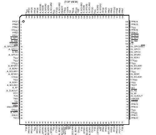
PinoutSpecificationsSupply voltage I/O range, DVDD‡ . . . . . . . . . . . . . . . . . . . . . . . . . .. . . . . . . . . . . . −0.3 V to 4.0 VSupply voltage core range, CVDD ‡. . . . . . . . . . . . . . . . . . . . . . . . . . . . . . . . . . . . −0.3 V to 2.4 VInput voltag...
TMS320VC5410: PinoutSpecificationsSupply voltage I/O range, DVDD‡ . . . . . . . . . . . . . . . . . . . . . . . . . .. . . . . . . . . . . . −0.3 V to 4.0 VSupply voltage core range, CVDD ‡. . ....
SeekIC Buyer Protection PLUS - newly updated for 2013!
268 Transactions
All payment methods are secure and covered by SeekIC Buyer Protection PLUS.
The TMS320VC5410 fixed-point, digital signal processor (DSP) (hereafter referred to as the TMS320VC5410 unless otherwise specified) is based on an advanced modified Harvard architecture that has one program memory bus and three data memory buses. This processor TMS320VC5410 provides an arithmetic logic unit (ALU) with a high degree of
parallelism, application-specific hardware logic, on-chip memory, and additional on-chip peripherals. The basis of the operational flexibility and speed of this DSP is a highly specialized instruction set.
Separate program and data spaces allow simultaneous access to program instructions and data, providing a high degree of parallelism. Two read operations and one write operation can be performed in a single cycle. Instructions with parallel store and application-specific instructions can fully utilize this architecture. In addition, data can be transferred between data and program spaces. Such parallelism supports a powerful set of arithmetic, logic, and bit-manipulation operations that can all be performed in a single machine cycle. The '5410 also includes the control mechanisms to manage interrupts, repeated operations, and function calls.
NOTE:This data sheet is designed to be used in conjunction with the TMS320C5000 DSP Family Functional Overview (literature number SPRU307).