TMS29VF040

Features: ` Single Power Supply 3.3 V ± 0.3 V TMS29LF040 2.7 V to 3.6 V TMS29VF040 5 V ± 10% See TMS29F040 Data sheet (Literature Number SMJS820)` Organization . . . 524288 By 8 Bits` Eight Equal Sectors of 64K Bytes Any Combination of Sectors Can Be ErasedAny Combination of Sectors Can Be Mark...

product image

TMS29VF040 Picture
SeekIC No. : 004524874 Detail

TMS29VF040: Features: ` Single Power Supply 3.3 V ± 0.3 V TMS29LF040 2.7 V to 3.6 V TMS29VF040 5 V ± 10% See TMS29F040 Data sheet (Literature Number SMJS820)` Organization . . . 524288 By 8 Bits` Eight Equal...

floor Price/Ceiling Price

Part Number:
TMS29VF040
Supply Ability:
5000

Price Break

  • Qty
  • 1~5000
  • Unit Price
  • Negotiable
  • Processing time
  • 15 Days
Total Cost: $ 0.00

SeekIC Buyer Protection PLUS - newly updated for 2013!

  • Escrow Protection.
  • Guaranteed refunds.
  • Secure payments.
  • Learn more >>

Month Sales

268 Transactions

Rating

evaluate  (4.8 stars)

Upload time: 2025/1/11

Payment Methods

All payment methods are secure and covered by SeekIC Buyer Protection PLUS.

Notice: When you place an order, your payment is made to SeekIC and not to your seller. SeekIC only pays the seller after confirming you have received your order. We will also never share your payment details with your seller.
Product Details

Description


Features:

` Single Power Supply 3.3 V ± 0.3 V TMS29LF040 2.7 V to 3.6 V TMS29VF040 5 V ± 10% See TMS29F040 Data sheet (Literature Number SMJS820)
` Organization . . . 524288 By 8 Bits
` Eight Equal Sectors of 64K Bytes Any Combination of Sectors Can Be ErasedAny Combination of Sectors Can Be Marked as Read-Only
` Compatible With JEDEC Electrically Erasable Programmable Read-Only Memory (EEPROM) Command Set
` Fully Automated On-Chip Erase and Byte-Program Operations
` 100000 Program/Erase Cycles
` Erase-Suspend/Erase-Resume Operation
` Compatible With JEDEC Byte-Wide Pinouts
` Low-Current Consumption Active Read . . . 20 mA Typical Active Program/Erase . . . 30 mA Typical
` All Inputs/Outputs CMOS-Compatible Only


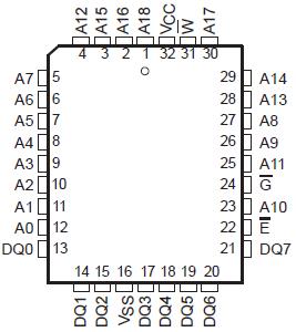
Pinout

  Connection Diagram


Specifications

Voltage range with respect to ground:
Supply voltage range, VCC (see Note 2) . . . . . . . . . . . . . . 0.5 V to + 3.6 V
All pins except A9, EG (see Note 2) . . . . . . . . . . . . . . . . . 0.5 V to + 3.6 V
A9, EG (see Note 3) . . . . . . . . . . . . . . . . . . . . . . . . . . . . 0.5 V to + 13.5 V
Ambient temperature range during read/erase/program, TA
Commercial (L) . . . . . . . . . . . . . . . . . . . . . . . . . . . . . . . . . . . . . . . 0 to 70
Extended (E) . . . . . . . . . . . . . . . . . . . . . . . . . . . . . . . . . . . . . . 40to 85
Storage temperature range, Tstg . . . . . . .  . . . . . . . . . . . . . . 65 to 150
† Stresses beyond those listed under "absolute maximum ratings" may cause permanent damage to the device. These are stress ratings only, and functional operation of the device at these or any other conditions beyond those indicated under "recommended operating conditions" is not implied. Exposure to absolute-maximum-rated conditions for extended periods may affect device reliability.
NOTES: 2. Minimum dc voltage on input or I/O pins is 0.5 V. D uring voltage transitions, input or I/O pins may undershoot VSS to 2.0 V for periods of up to 20 ns. Maximum dc voltage on input and I/O pins is +3.6 V. During voltage transitions, input and I/O pins may overshoot to VCC + 2.0 V for periods up to 20 ns.
3. Minimum dc input voltage on A9, E, and G pins is 0.5 V. During voltage transitions, A9,E, and G may undershoot VSS to 2.0 V for periods of up to 20 ns. Maximum dc input voltage on A9, E, and G pins is +12.5 V, which may overshoot to +13.5 V for periods up to 20 ns.


Description

The TMS29LF040 and TMS29VF040 are 524288 by 8-bit (4194304-bit), low-voltage, single-supply,programmable read-only memories that can be erased electrically and reprogrammed. These devices are organized as eight independent 64K-byte sectors and are offered with access times between 80 ns and 150 ns.

An on-chip state machine controls the program and erase operations. The embedded-byte program and sector/chip-erase functions are fully automatic. The command set is compatible with that of JEDEC 4M-bit EEPROMs. A suspend/resume feature allows access to unaltered memory sectors during a sector-erase operation. Data protection of any sector combination is accomplished using a hardware sector-protection feature.

Device operations are selected by writing JEDEC-standard commands into the command register using standard microprocessor-write timings. The command register acts as input to an internal state machine that interprets the commands, controls the erase and programming operations, and outputs the status of the device, the data stored in the device, and the device algorithm-selection code. On initial power-up operation, the device defaults to the read mode.

The TMS29xF040 is offered in a 32-pin 8 x 14 mm thin small-outline package (DBW suffix), a 32-pin 8 x 20 mm thin small-outline package (DD suffix), and a 32-pin plastic leaded chip carrier (FM suffix) using 1.27 mm (50-mil) lead pitch


Customers Who Bought This Item Also Bought

Margin,quality,low-cost products with low minimum orders. Secure your online payments with SeekIC Buyer Protection.
Power Supplies - Board Mount
Power Supplies - External/Internal (Off-Board)
LED Products
Crystals and Oscillators
View more