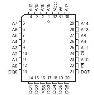
Features: `Single Power Supply: 5 V ± 10% 3.3 V ± 0.3 V See TMS29LF040/ TMS29VF040 Data Sheet (Literature Number SMJS825) 2.7 V to 3.6 V See TMS29LF040/ TMS29VF040 Data Sheet
`Organization . . . 524288 By 8 Bits
`Eight Equal Sectors of 64K Bytes Any Combination of Sectors Can Be Erased Any Combination of Sectors Can Be Marked as Read-Only
`Compatible With JEDEC Electrically Erasable Programmable Read-Only Memory (EEPROM) Command Set
`Fully Automated On-Chip Erase and Byte-Program Operations
`100000 Program/Erase Cycles
`Erase-Suspend/Erase-Resume Operation
`Compatible With JEDEC Byte-Wide Pinouts
`Low-Current Consumption Active Read . . . 20 mA Typical Active Program/Erase . . . 30 mA Typical
`All Inputs/Outputs TTL-Compatible
Pinout Specifications
Voltage range with respect to ground:
Supply voltage range, VCC (see Note 2) . . . . . . . . . . . . . . . . . . . . . . . 2.0 V to +7.0 V
All pins except A9, E, G (see Note 2) . . . . . . . . . . . . . . . . . . . . . . . . 2.0 V to +7.0 V
A9, E, G (see Note 3) . . . . . . . . . . . . . . . . . . . . . . . . . . . . . . . . . . . . . 2.0 V to +13.5 V
Ambient temperature range during read/erase/program, TA
Commercial (L) . . . . . . . . . . . . . . . . . . . . . . . . . . . . . . . . . . . . . . . 0°C to 70°C
Extended (E) . . . . . . . . . . . . . . . . . . . . . . . . . . . . . . . . . . . . . . . 40°C to 85°C
Storage temperature range, Tstg . . . . . . . . . . . . . . . . . . . . . . . . . . . . . . . . . . . . . . . . . . . . . . . . . . . 65°C to 150°C
† Stresses beyond those listed under "absolute maximum ratings" may cause permanent damage to the device. These are stress ratings only, and functional operation of the device at these or any other conditions beyond those indicated under "recommended operating conditions" is not implied. Exposure to absolute-maximum-rated conditions for extended periods may affect device reliability.
NOTES:
2. Minimum dc voltage on input or I/O pins is 0.5V. During voltage transitions, input or I/O pins may undershoot VSS to 2.0 V for periods of up to 20 ns. Maximum dc voltage on input and I/O pins is VCC + 0.5V. During voltage transitions, input and I/O pins may overshoot to VCC + 2.0 V for periods up to 20 ns.
3. Minimum dc input voltage on A9, E, and G pins is 0.5 V. During voltage transitions, A9, E, and G may undershoot VSS to 2.0 V for periods of up to 20 ns. Maximum dc input voltage on A9, E, and G pins is +12.5 V, which may overshoot to +13.5 V for periods up to 20 ns.
DescriptionThe TMS29F040 is a 524288 by 8-bit (4194304-bit), 5-V single-supply, programmable read-only memory that can be electrically erased and reprogrammed. This device is organized as eight independent 64K-byte sectors and is offered with access times between 60 ns and 120 ns.
An on-chip state machine controls the program and erase operations. The embedded byte-program and sector/chip-erase functions are fully automatic. The command set is compatible with that of JEDEC 4M-bit EEPROMs. A suspend/resume feature allows access to unaltered memory sectors during a sector-erase operation. Data-protection of any sector combination is accomplished using a hardware sector-protection feature.
Device operations are selected by writing JEDEC-standard commands into the command register using standard microprocessor write timings. The command register acts as input to an internal-state machine that interprets the commands, controls the erase and programming operations, and outputs the status of the device, the data stored in the device, and the device algorithm-selection code. On initial power-up operation, the device defaults to the read mode.
The TMS29F040 is offered in a 32-pin plastic leaded chip carrier (FM suffix) using 1.27-mm (50-mil) lead pitch and a 32-pin thin small-outline package (DD suffix).

 TMS29F040 Data Sheet


