Features: `Organization . . . 524288 By 8 Bits 262144 By 16 Bits
` Array-Blocking Architecture One 16K-Byte Protected Boot Block Two 8K-Byte Parameter Blocks One 96K-Byte Main Block Three 128K-Byte Main Blocks Top or Bottom Boot Locations
` '28F400Axy Offers a User-Defined 8-Bit (Byte) or 16-Bit (Word) Organization
` '28F004Axy Offers Only the 8-Bit Organization
` Maximum Access/Minimum Cycle Time Commercial and Extended 5-V VCC ± 10% 3.3-V VCC ± 0.3 V '28F400Axy60 60 ns 110 ns '28F400Axy70 70 ns 130ns '28F400Axy80 80 ns 150 ns Automotive (offered for only 5-V VCC voltage configurations) 5-V VCC ± 10% '28F400Axy70 70 ns '28F400Axy80 80 ns '28F400Axy90 90 ns (x = S, E, F, M, or Z Depending on VCC/VPP Configuration) (y = T or B for Top or Bottom Boot-Block Configuration)
` 100000 and 10000 Program/Erase Cycle Versions
`Three Temperature Ranges Commercial . . . 0°C to 70°C Extended . . . 40°C to 85°C Automotive . . . 40°C to 125°C
` Industry Standard Packages Offered in 40-Pin TSOP (DCD Suffix) 44-Pin PSOP (DBJ Suffix) 48-Pin TSOP (DCD Suffix)
`Low Power Dissipation (VCC = 5.5 V) Active Write . . . 248 mW (Byte Write) Active Read . . . 330 mW (Byte Read) Active Write . . . 248 mW (Word Write) Active Read . . . 330 mW (Word Read) Block Erase . . . 165 mW Standby . . . 0.72 mW (CMOS-Input Levels)
` Fully Automated On-Chip Erase and Word/Byte Program Operations
` Write Protection for Boot Block
` Industry Standard Command-State Machine (CSM) Erase Suspend/Resume Algorithm-Selection Identifier
` Three Different Combinations of Supply Voltages Offered
` All Inputs/Outputs TTL Compatible
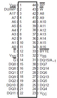
Pinout Specifications
Supply voltage range, VCC (see Note 4) . . . . . . . . . . . . . . . . . . . . . . . . . . . . . . . . . . . . . . . . . . . . . . 0.6 V to 7 V
Supply voltage range, VPP (see Note 4) . . . . . . . . . . . . . . . . . . . . . . . . . . . . . . . . . . . . . . . . . . . . . 0.6 V to 14 V
Input voltage range: All inputs except A9, RP . . . . . . . . . . . . . . . . . . . . . . . . . . . . . . . . . . . 0.6 V to VCC + 1 V
RP, A9 (see Note 5) . . . . . . . . . . . . . . . . . . . . . . . . . . . . . . . . . . . . . . . . . . 0.6 V to 13.5 V
Output voltage range (see Note 6) . . . . . . . . . . . . . . . . . . . . . . . . . . . . . . . . . . . . . . . . . . . . . 0.6 V to VCC + 1 V
Operating free-air temperature range, TA, during read/erase/program: L suffix . . . . . . . . . . . . . . 0°C to 70°C
E suffix . . . . . . . . . . . . 40°C to 85°C
Q suffix . . . . . . . . . . 40°C to 125°C
Storage temperature range, Tstg . . . . . . . . . . . . . . . . . . . . . . . . . . . . . . . . . . . . . . . . . . . . . . . . . . 65°C to 150°C
† Stresses beyond those listed under "absolute maximum ratings" may cause permanent damage to the device. These are stress ratings only, and functional operation of the device at these or any other conditions beyond those indicated under "recommended operating conditions" is not implied. Exposure to absolute-maximum-rated conditions for extended periods may affect device reliability.
NOTES:
1. All voltage values are with respect to VSS.
2. The voltage on any input or output can undershoot to 2 V for periods less than 20 ns. See Figure 8.
3. The voltage on any input or output can overshoot to 7 V for periods less than 20 ns. See Figure 9.
DescriptionThe TMS28F400Axy is a 524288 by 8 bits/262144 by 16 bits (4194304-bit), boot-block flash memory that can be electrically block-erased and reprogrammed. The TMS28F400Axy is organized in a blocked architecture consisting of:
· One 16K-byte protected boot block
· Two 8K-byte parameter blocks
· One 96K-byte main block
· Three 128K-byte main blocks
Table 1 lists the five different voltage configurations available for ordering. Operation as a 512K-byte (8-bit) or a 256K-word (16-bit) organization is user-definable.

 TMS28F004Axy Data Sheet


