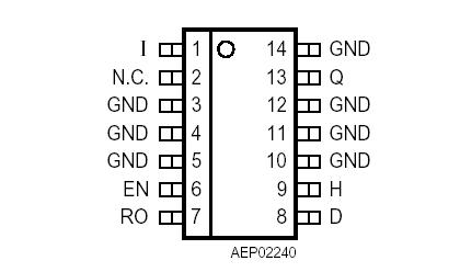
Features: Features• Output voltage tolerance ± 2%• Very low standby current consumption• Input voltage up to 42 V• Reset function down to 1 V output voltage• ESD protection up to 2000 V• Adjustable reset time• On/Off logic• Overtemperature protectio...
TLE 4287 G: Features: Features• Output voltage tolerance ± 2%• Very low standby current consumption• Input voltage up to 42 V• Reset function down to 1 V output voltage• ESD prote...
SeekIC Buyer Protection PLUS - newly updated for 2013!
268 Transactions
All payment methods are secure and covered by SeekIC Buyer Protection PLUS.
Features: • Drives motors up to 2 A• Integrated free-wheeling diodes 2.5 A• Shor...
Parameter | Symbol | Limit Values | Unit | Remarks | |
min. | max. | ||||
Input | |||||
Voltage | VL |
-0.5 | 42 | V | - |
Current | II | - | - | mA | internally limited |
Output Q | |||||
Voltage | VQ |
-0.3 | 7 | V | |
Current | IQ | - | - | A | - |
Reset Output | |||||
Voltage | VR | -0.3 | 7 | V | - |
Current | IR | - | - | - |
internally limited |
Reset Delay D | |||||
Voltage | VD | -0.3 | 42 | V | |
Current | ID | - | - | - | internally limited |
Enable EN | |||||
Voltage | VEN | - 42 | 42 | V | |
Current | IEN | -5 | 5 | mA | -t400ms |
Functional Description
The TLE 4287 G is a monolithic integrated 5 V voltage regulator in P-DSO-14-8 package. It supplies an output current IQ > 250 mA. The IC is short circuit proof and incorporates temperature protection which turns off the device at overtemperature. The input voltage VI is regulated in the range of 7.5 V < VI < 40 V to VQ,nom = 5 V. Therefore a reference voltage, which is kept highly accurate by resistance adjustment, is compared via a control amplifier to a voltage that is proportional to the output voltage. The control amplifier drives the base of the series transistor by a buffer.
A comparator in the reset-generator block TLE 4287 G compares a reference voltage that is independent of the input voltage to the scaled-down output voltage. In the case of an output voltage VQ < 4.5 V the reset delay capacitor is discharged and a reset signal is generated by setting the reset output LOW. The reset delay time can be set by choosing the external capacitor over a wide range. When the output voltage rises above VQ 4.5 V the reset delay capacitor is charged again. As soon as the delay capacitor voltage reaches the upper switching threshold the reset output pin is set HIGH again.