Supply Current
:
Operating Temperature Range
:
Packaging
: Reel
Operating Supply Voltage
: 5 V
Type
: Transceiver
Package / Case
: DSO
Features: • Standard fault tolerant differential CAN-transceiver
• Bus failure management
• Low power mode management
• CAN data transmission rate up to 125 kBaud
• Low-dropout voltage 5 V regulator for internal
and external supply; tolerance ± 2%
• High Side Switche
• Power on and under-voltage reset generator
• Window watchdog
• Programable time base
• Standard 8 bit SPI-Interface
• Wide input voltage range
• Wide temperature range
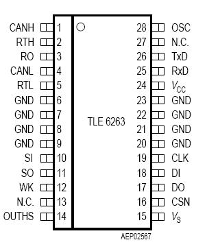
• Enhanced power P-DSO-PackagePinout Specifications
| Parameter |
Symbol |
Limit Values |
Unit |
Notes |
| min. |
max. |
| Voltages |
| Supply voltage |
VS |
0.3 |
28 |
V |
- |
| Supply voltage |
VS |
0.3 |
40 |
V |
tp< 0.5 s; tp/T < 0.1 |
| Regulator output voltage |
VCC |
0.3 |
5.5 |
V |
- |
CAN input voltage (CANH,
CANL) |
VCANH/L |
10 |
27 |
V |
- |
CAN input voltage
(CANH, CANL) |
VCANH/L |
40 |
40 |
V |
VS >0 V
tp< 0.5 s; tp/T < 0.1 |
Logic input voltages (DI, CLK,
CSN, OSC, TxD) |
VI |
0.3 |
VCC
+ 0.3 |
V |
0 V < VS < 24 V
0 V < VCC < 5.5 V |
Logic output voltage
(DO, RO, SO, RxD) |
VDRSO,R |
0.3 |
VCC
+ 0.3 |
V |
0 V < VS < 24 V
0 V < VCC < 5.5 V |
Termination input voltage
(RTH, RTL) |
VTL /TH |
0.3 |
VS
+ 0.3 |
V |
0 V < VS < 24 V
0 V < VCC < 5.5 V |
| Input voltages at WK and SI |
VWK/SI |
0.3 |
28 |
V |
- |
| Input voltages at WK and SI |
VWK/SI |
0.3 |
40 |
V |
tp< 0.5 s; tp/T < 0.1 |
| Currents |
| Output current; VCC |
ICC |
- |
- |
A |
internally limited |
| Output current; OUTHS |
IOUTH1 |
* |
0.2 |
A |
* internally limited |
| Temperatures |
| Junction temperature |
Tj |
40 |
150 |
°C |
- |
| Storage temperature |
Tstg |
50 |
150 |
°C |
- |
Note: Maximum ratings are absolute ratings; exceeding any one of these values may
cause irreversible damage to the integrated circuit.DescriptionThe TLE6263G is a monolithic integrated circuit in a P-DSO-28-6 package, which incorporates a failure tolerant low speed CAN-transceiver for differential mode data transmission, a low dropout voltage regulator for internal and external 5V supply as well as a SPI (serial peripheral interface) to control and monitor the IC. Further there are integrated a high side switch, a wake-up input, a window watchdog circuit as well as a reset and early warning feature. Both, the window watchdog and reset function are referring to a time base that is programmable via an external resistor. The IC is designed to withstand the severe conditions of automotive applications.
The features of TLE6263G are (1)standard fault tolerant differential CAN-transceiver; (2)bus failure management; (3)low power mode management; (4)CAN data transmission rate up to 125 kBaud; (5)low-dropout voltage 5 V regulator for internal and external supply; tolerance ± 2%; (6)high Side Switche; (7)power on and under-voltage reset generator; (8)window watchdog; (9)programable time base; (10)standard 8 bit SPI-Interface; (11)wide input voltage range; (12)wide temperature range; (13)enhanced power P-DSO-Package. The TLE 6263 G is a monolithic IC, which incorporates a failure tolerant low speed CAN-transceiver for differential mode data transmission, a low dropout voltage regulator for internal and external 5 V supply as well as a SPI (serial periperal interface) to control and monitor the IC. Further there are integrated a high side switche, a wake-up input, a window watchdog circuit as well as a reset circuit and early warning function. Both, the window watchdog and reset function are referring to a time base that is programmable via an external resistor.
The absolute maximum ratings of TLE6263G are (1)supply voltage(VS): -0.3 to 28V; (2)supply voltage(VS): -0.3 to 40V(@tp< 0.5s; tp/T < 0.1); (3)regulator output voltage(VCC):-0.3 to 5.5 V; (4)CAN input voltage (CANH, CANL) (VCANH/L): -10 to 27V; (5)CAN input voltage(CANH, CANL)(VCANH/L): -40 to 40V (@ VS >0 V tp< 0.5s; tp/T < 0.1); (6)logic input voltages (DI, CLK, CSN, OSC, PWM, TxD)(VI): -0.3 to VCC +0.3V (@0 V < VS < 24 V; 0 V < VCC < 5.5 V); (7)logic output voltage (DO, RO, RxD)(VDO/RO/RD): -0.3 to VCC +0.3V(@ 0 V < VS < 24 V; 0 V < VCC < 5.5 V); (8)termination input voltage (RTH, RTL)(VTL /TH) of the TLE6263G: -0.3 to VS +0.3V (@0 V < VS < 24 V; 0 V < VCC < 5.5 V); (9) input voltages at WK and SI(VWK/SI): 0.3 to 28V; (10) input voltages at WK and SI (VWK/SI): -0.3 to 40V (@tp< 0.5 s; tp/T < 0.1); (11) junction temperature(Tj): -40 to 150 °C;(12) storage temperature(Tstg): -50 to 150°C.(Note: Maximum ratings are absolute ratings; exceeding any one of these values may cause irreversible damage to the integrated circuit.)

 TLE6263G Data Sheet


