TLC2810Z

PinoutSpecificationsSupply voltage, VCC(see Note 1) . . . . . . . . . . . . . . . . . . . . . . . . . . . . . . . . . . . . .±16.5 VSupply voltage, VDD (see Note 2). . . . . . . . . . . . . . . . . . . . . . . . . . . . . . . . . .. . . .±5.5 VInput voltage, VI (any input). . . . . . . . . . . . ....

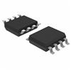
product image

TLC2810Z Picture
SeekIC No. : 004520543 Detail

TLC2810Z: PinoutSpecificationsSupply voltage, VCC(see Note 1) . . . . . . . . . . . . . . . . . . . . . . . . . . . . . . . . . . . . .±16.5 VSupply voltage, VDD (see Note 2). . . . . . . . . . . . . . . . . ...

floor Price/Ceiling Price

Part Number:
TLC2810Z
Supply Ability:
5000

Price Break

  • Qty
  • 1~5000
  • Unit Price
  • Negotiable
  • Processing time
  • 15 Days
Total Cost: $ 0.00

SeekIC Buyer Protection PLUS - newly updated for 2013!

  • Escrow Protection.
  • Guaranteed refunds.
  • Secure payments.
  • Learn more >>

Month Sales

268 Transactions

Rating

evaluate  (4.8 stars)

Upload time: 2025/1/11

Payment Methods

All payment methods are secure and covered by SeekIC Buyer Protection PLUS.

Notice: When you place an order, your payment is made to SeekIC and not to your seller. SeekIC only pays the seller after confirming you have received your order. We will also never share your payment details with your seller.
Product Details

Description


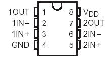
Pinout

  Connection Diagram


Specifications

Supply voltage, VCC(see Note 1) . . . . . . . . . . . . . . . . . . . . . . . . . . . . . . . . . . .  . .±16.5 V
Supply voltage, VDD (see Note 2). . . . . . . . . . . . . . . . . . . . . . . . . . . . . . . . .  .. . . .±5.5 V
Input voltage, VI (any input). . . . . . . . . . . . . . . . . . . . . . . . . . . . . . . . . . .  . . . . .. . . . VCC
Input current, II . . . . . . . . . . . . . . . . . . . . . . . . . . . . . . . . . . . . . . . . . . . . .. . ..  . . .±2 mA
Output current, IO . . . . . . . . . . . . . . . . . . . . . . . . . . . . . . . . . . . . .  . . . . . . .. .  . .250 mA
Total current into VDD . . . . . . . . . . . . . . . . . . . . . . . . . . . . .. . . . . . . . . . . . . . . . . . .45 mA
Total current out of GND  . . . . . . . . . . . . . . . . . . . . . . . . . . . . . . . . . . . . . . . . . . . . .45 mA
Duration of short-circuit current at (or below) TA = 25°C (see Note 3)  . . . . . . .unlimited

Continuous total power dissipation . . . . . . . . . . . . . . .. . .   .See Dissipation Rating Table
Operating free-air temperature, TA . . . . . . . . . . . . . . . . . . . .. . . ..   . ..40°C to 150°C                                                      
Storage temperature, Tstg . . . . . . . . . . . . . . . . . . . . . . . . . . . . .. . . . .65°C to 165°C
Lead temperature 1,6 mm (1/16 Inch) from case for 10 seconds . . . . . . . . .. .. . .260°C

NOTES: 1. All voltage values, except differential voltages, are with respect to network ground.
2. Differential voltages are at IN+ with respect to IN .
3. The output may be shorted to either supply. Temperature and/or supply voltages must be limited to ensure that the maximum
dissipation rating is not exceeded (see application selection).


Description

The TLC2810Z dual operational amplifiers combine low offset voltage drift with high input impedance, low noise, and speeds approaching that of general-purpose JFET devices. In addition, the use of Texas Instruments silicon-gate LinCMOS technology assures offset stability that greatly exceeds the stability available with conventional metal-gate processes.

The high input impedance, low bias current, and high slew rate make the TLC2810Z ideal for applications that have previously been reserved for JFET and NFET products. These advantages, in combination with an upper operating temperature of 150°C, make the TLC2810Z an ideal choice for precision, extremely high-temperature

applications. In general, many features associated with bipolar technology are available on the TLC2810Z without the power penalties of bipolar technology. General applications such as transducer interfacing, analog calculations, amplifier blocks, active filters, and signal buffering are designed easily with the TLC2810Z.

The TLC2810Z package options include a small-outline version for high-density system applications.

The device inputs and outputs are designed to withstand 100-mA surge currents without sustaining latch-up at 25°C. The TLC2810Z incorporates internal ESD-protection circuits that prevent functional failures at voltages up to 2000 V as tested under MIL-STD 883C, Method 3015.2. However, care should be exercised in handling the TLC2810Z as exposure to ESD may result in the degradation of the device parametric performance. Additional care should be exercised to prevent VDD supply line transients under power conditions. Transients of greater than 20 V can trigger the ESD-protection structure, inducing a low-impedance path to GND. Should
this condition occur, the sustained current supplied to the device must be limited to 100 mA or less. Failure to do so can result in a latched condition and device failure.
The TLC2810Z is characterized for operation over the extended temperature range from 40°C to 150°C.


Customers Who Bought This Item Also Bought

Margin,quality,low-cost products with low minimum orders. Secure your online payments with SeekIC Buyer Protection.
Prototyping Products
DE1
Transformers
Cable Assemblies
Semiconductor Modules
Computers, Office - Components, Accessories
Audio Products
View more