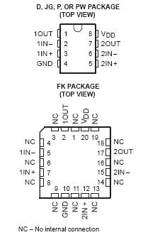
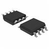
Features: Trimmed Offset Voltage: TLC277 . . . 500 V Max at 25°C, VDD = 5 VInput Offset Voltage Drift . . . Typically 0.1 V/Month, Including the First 30 DaysWide Range of Supply Voltages Over Specified Temperature Range: 0°C to 70°C . . . 3 V to 16 V 40°C to 85°C . . . 4 V to 16 V 55°C to 125°C ....
TLC272: Features: Trimmed Offset Voltage: TLC277 . . . 500 V Max at 25°C, VDD = 5 VInput Offset Voltage Drift . . . Typically 0.1 V/Month, Including the First 30 DaysWide Range of Supply Voltages Over Speci...
SeekIC Buyer Protection PLUS - newly updated for 2013!
268 Transactions
All payment methods are secure and covered by SeekIC Buyer Protection PLUS.
US $1.83 - 2.88 / Piece
Operational Amplifiers - Op Amps Advanced LinCMOS Low-Noise Precision
US $1.83 - 2.88 / Piece
Operational Amplifiers - Op Amps Advanced LinCMOS Low-Noise Precision
The TLC272 and TLC277 precision dual operational amplifiers combine a wide range of input offset voltage grades with low offset voltage drift, high input impedance, low noise, and speeds approaching that of general-purpose BiFET devices.
These devices TLC272 and TLC277 use Texas instruments silicon-gate LinCMOSE technology, which provides offset voltage stability far exceeding the stability available with conventional metal-gate processes.
The extremely high input impedance, low bias currents, and high slew rates make these costeffective devices ideal for applications which have previously been reserved for BiFET and NFET products. Four offset voltage grades are available (C-suffix and I-suffix types), ranging from the low-cost TLC272 (10 V) to the high-precision TLC277 (500 V). These advantages, in combination with good common-mode rejection and supply voltage rejection, make these devices a good choice for new state-of-the-art designs as well as for upgrading existing designs.