Output Current
:
Number of Channels
: 1
Mounting Style
: SMD/SMT
Maximum Operating Temperature
: + 125 C
Package / Case
: SOIC-8
Packaging
: Tube
Common Mode Rejection Ratio (Min)
: 120 dB
Shutdown
: No
Input Bias Current (Max)
: 60 pA
Operating Supply Voltage
: 16 V
Slew Rate
: 2.8 V/us
Input Offset Voltage
: 0.0035 mV
Pinout Description
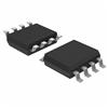
The TLC2652Q-8D is high-precision chopper-stabilized operational amplifiers using Texas Instruments Advanced LinCMOSE process. The features of TLC2652Q-8D are: (1)Extremely Low Offset Voltage: 1 V Max; (2)Extremely Low Change on Offset Voltage With Temperature: 0.003 V/°C Typ; (3)Low Input Offset Current 500 pA Max at TA = 55°C to 125°C; (4)AVD: 135 dB Min; (5)CMRR and kSVR:120 dB Min; (6)Single-Supply Operation; (7)Common-Mode Input Voltage Range Includes the Negative Rail; (8)No Noise Degradation With External Capacitors Connected to VDD
The following is about the absolute maximum ratings of TLC2652Q-8D: (1)Supply voltage VDD+: 8 V; (2)Supply voltage VDD: 8 V; (3)Differential input voltage, VID: ±16 V; (4)Input voltage, VI: ±8 V; (5)Voltage range on CLK IN and INT/EXT: VDD to VDD + 5.2 V; (6)Input current, II (each input): ±5 mA; (7)Output current, IO: ±50 mA; (8)Duration of short-circuit current at (or below) 25°C: unlimited; (9)Current into CLK IN and INT/EXT: ±5 mA; (10)Continuous total dissipation: See Dissipation Rating Table; (11)Operating free-air temperature range, TA: C suffix: 0°C to 70°C.
The electrical characteristics of the TLC2652Q-8D are: (1)input offset voltage: 0.6V typ and 3V max; (2)temperature coefficient of input offset voltage: 4.35V max; (3)input offset voltage long-term drift: 0.033V/ typ and 0.03V/ max ; (4)input offset current: 2pA typ; (5)input bias current: 4pA typ; (6)common-mode input voltage range: -5V to 3.1V min; (7)maximum positive peak output voltage swing: 4.7V min and 4.8V typ; (8)maximum negative peak output voltage swing: -4.7V min and -4.9V typ.

 TLC2652Q-8D Data Sheet


