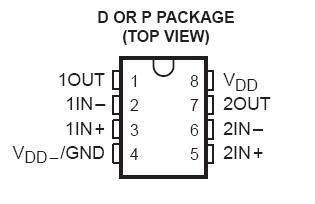
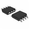
Features: A-Suffix Versions Offer 5-mV VIO
B-Suffix Versions Offer 2-mV VIO
Wide Range of Supply Voltages 1.4 V to 16 V
True Single-Supply Operation
Common-Mode Input Voltage Includes the Negative Rail
Low Noise . . . 30 nV//Hz Typ at f = 1 kHz (High-Bias Versions)Pinout SpecificationsSupply voltage, VDD (see Note 1) . . . . . . . . . . . . . . . . . . . . . . . . . . . . . . . .. . . .. . . 18 V
Differential input voltage, VID (see Note 2) . . . . . . . . . . . . . . . . . . . . . . . . . . . . . .. . ±18 V
Input voltage range, VI (any input) . . . . . . . . . . . . . . . . . . . . . . . . . . . . .. . . . . . . . 0.3 V to 18 V
Duration of short circuit at (or below) 25°C free-air temperature (see Note 3 . . .. . unlimited
Continuous total dissipation . . . . . . . . . . . . . . . . . . . . . . . . . . . . . . . . . . . . . . . . . . . See Dissipation Rating Table
Operating free-air temperature range, TA . . . . . . . . . . . . . . . . . . . . . . . . . . . . .. . . . 0°C to 70°C
Storage temperature range . . . . . . . . . . . . . . . . . . . . . . . . . . . . . . . . . . . . . . . . . . 65°C to 150°C
Lead temperature 1,6 mm (1/16 inch) from case for 10 seconds . . . . . . .. . . . . . . . . 260°C
† Stresses beyond those listed under "absolute maximum ratings" may cause permanent damage to the device. These are stress ratings only, and functional operation of the device at these or any other conditions beyond those indicated under "recommended operating conditions" is not implied. Exposure to absolute-maximum-rated conditions for extended periods may affect device reliability.
NOTES: 1. All voltage values, except differential voltages, are with respect to VDD/GND.
2. Differential voltages are at IN+, with respect to IN .
3. The output may be shorted to either supply. Temperature and/or supply voltages must be limited to ensure the maximum dissipation rating is not exceeded.DescriptionThe TLC252, TLC25L2, and TLC25M2 are low-cost, low-power dual operational amplifiers designed to operate with single or dual supplies. These devices TLC252, TLC25L2, and TLC25M2 utilize the Texas Instruments silicon gate LinCMOSE process, giving them stable input offset voltages that are available in selected grades of 2, 5, or 10 mV maximum, very high input impedances, and extremely low input offset and bias currents. Because the input common-mode range extends to the negative rail and the power consumption is extremely low, this series is ideally suited for battery-powered or energy-conserving applications. The series offers operation down to a 1.4-V supply, is stable at unity gain, and has excellent noise characteristics.
These devices TLC252, TLC25L2, and TLC25M2 have internal electrostatic-discharge (ESD) protection circuits that prevent catastrophic failures at voltages up to 2000 V as tested under MIL-STD-883C, Method 3015.1. However, care should be exercised in handling these devices as exposure to ESD may result in a degradation of the device parametric performance.

 TLC25M2B Data Sheet


