Maximum Power Dissipation
:
Architecture
: SAR
Supply Voltage - Max
: 5.5 V
Mounting Style
: SMD/SMT
Packaging
: Tube
Input Type
: Voltage
Resolution
: 12 bit
Maximum Operating Temperature
: + 85 C
Number of Converters
: 1
Package / Case
: SOIC-16
Supply Voltage - Min
: 4.5 V
SNR
: 69 dB
Conversion Rate
: 400 KSPs
Voltage Reference
: Internal, External
Interface Type
: 4-Wire, Serial, SPI
Number of ADC Inputs
: 4, 3
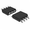
DescriptionThe TLC2554ID is designed as one member of the TLC2554 family of high-performance, 12-bit low power, 1.6 ms, CMOS analog-to-digital converters (ADC) which operate from a single 5 V power supply. This TLC2554ID family has three digital inputs and a 3-state output [chip select (CS), serial input-output clock (SCLK), serial data input (SDI), and serial data output (SDO)] that provide a direct 4-wire interface to the serial port of most popular host microprocessors (SPI interface). When interfaced with a DSP, a frame sync (FS) signal is used to indicate the start of a serial data frame.
TLC2554ID has twelve features. (1)Maximum throughput 400 KSPS. (2)Built-in reference and 8× FIFO. (3)Differential / integral nonlinearity error ±1 LSB. (4)Signal-to-noise and distortion ratio: 69 dB, fi = 12 kHz. (5)Spurious free dynamic range: 75 dB, fi = 12 kHz. (6)SPI/DSP-compatible serial interfaces with SCLK up to 20 MHz. (7)Single supply 5 Vdc. (8)Analog input range 0V to supply voltage with 500 kHz BW. (9)Hardware controlled and programmable sampling period. (10)Low operating current (4 mA at 5.5V external ref, 6mA at 5.5V, internal ref). (11)Power down: software/hardware power-down mode (1mA max, ext ref), auto power-down mode (1 mA, ext ref). (12)Programmable auto-channel sweep. That are all the main features.
Some absolute maximum ratings of TLC2554ID have been concluded into several points as follow. (1)Its supply voltage range, GND to VCC would be from -0.3V to 6.5V. (2)Its analog input voltage range would be from -0.3V to VCC + 0.3V. (3)Its reference input voltage would be VCC + 0.3V. (4)Its digital input voltage range would be from -0.3V to VCC + 0.3V. (5)Its operating virtual junction temperature range would be from -40°C to 150°C. (6)Its operating free-air temperature range would be from -40°C to 85°C. (7)Its storage temperature range would be from -65°C to 150°C. (8)Its lead temperature 1,6 mm (1/16 inch) from case for 10 seconds would be 260°C. It should be noted that stresses above those listed in absolute maximum ratings may cause permanent damage to device. And so on. If you have any question or suggestion or want to know more information please contact us for details. Thank you!
Parameters: | Technical/Catalog Information | TLC2554ID |
| Vendor | Texas Instruments |
| Category | Integrated Circuits (ICs) |
| Number of Bits | 12 |
| Package / Case | 16-SOIC (3.9mm Width) |
| Data Interface | Serial |
| Packaging | Tube |
| Sampling Rate (Per Second) | 200k |
| Operating Temperature | -40°C ~ 85°C |
| Voltage Supply Source | Single |
| Number of Inputs and Type | 4 Single-Ended, Unipolar; 2 Pseudo-Differential, Unipolar |
| Number of Converters | 1 |
| Power Dissipation (Max) | 9.5mW |
| Drawing Number | 296; 4040047-4; D; 16 |
| Lead Free Status | Lead Free |
| RoHS Status | RoHS Compliant |
| Other Names | TLC2554ID
TLC2554ID
296 2913 5 ND
29629135ND
296-2913-5
|

 TLC2554ID Data Sheet


