TLC2543C

Features: 12-Bit-Resolution A/D Converter10-ms Conversion Time Over Operating Temperature11 Analog Input Channels3 Built-In Self-Test ModesInherent Sample-and-Hold FunctionLinearity Error . . . ±1 LSB MaxOn-Chip System ClockEnd-of-Conversion OutputUnipolar or Bipolar Output Operation (Signed Binar...

product image

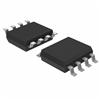
TLC2543C Picture
SeekIC No. : 004520470 Detail

TLC2543C: Features: 12-Bit-Resolution A/D Converter10-ms Conversion Time Over Operating Temperature11 Analog Input Channels3 Built-In Self-Test ModesInherent Sample-and-Hold FunctionLinearity Error . . . ±1 L...

floor Price/Ceiling Price

Part Number:
TLC2543C
Supply Ability:
5000

Price Break

  • Qty
  • 1~5000
  • Unit Price
  • Negotiable
  • Processing time
  • 15 Days
Total Cost: $ 0.00

SeekIC Buyer Protection PLUS - newly updated for 2013!

  • Escrow Protection.
  • Guaranteed refunds.
  • Secure payments.
  • Learn more >>

Month Sales

268 Transactions

Rating

evaluate  (4.8 stars)

Upload time: 2025/1/11

Payment Methods

All payment methods are secure and covered by SeekIC Buyer Protection PLUS.

Notice: When you place an order, your payment is made to SeekIC and not to your seller. SeekIC only pays the seller after confirming you have received your order. We will also never share your payment details with your seller.
Product Details

Description


Features:

 12-Bit-Resolution A/D Converter
 10-ms Conversion Time Over Operating Temperature
 11 Analog Input Channels
 3 Built-In Self-Test Modes
 Inherent Sample-and-Hold Function
 Linearity Error . . . ±1 LSB Max
 On-Chip System Clock
 End-of-Conversion Output
 Unipolar or Bipolar Output Operation (Signed Binary With Respect to 1/2 the Applied Voltage Reference)
 Programmable MSB or LSB First
 Programmable Power Down
 Programmable Output Data Length
 CMOS Technology
 Application Report Available†


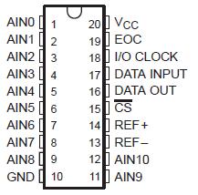
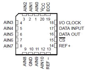
Pinout

  Connection Diagram  Connection Diagram


Specifications

Supply voltage range, VCC (see Note 1)  . . . . . . . . . .  . . . . . . .  .  0.5 V to 6.5 V
Input voltage range, VI (any input) . . . . . . . . . .. .  . . . .   .  0.3 V to VCC + 0.3 V
Output voltage range, VO . . ..  . . . . . . . . . . . . . .  . . . .  . . .0.3 V to VCC + 0.3 V
Positive reference voltage, Vref+ .. . . . . . . . . . . . . . . . . . .  . . . .  .  ... VCC + 0.1 V
Negative reference voltage, Vref . . . . . . . . . . . . . . . . . . . . . .  . . . .  . . .. 0.1 V
Peak input current, II (any input) . . . . . . . . . . . . . . . . . . . . . . . . . .  . .  . . ±20 mA
Peak total input current, II (all inputs) .. . . . . .. . . . . . . . . .  . . . .   . .. . . . ±30 mA
Operating free-air temperature range, TA: TLC2543C . .  . . . .  .  ... 0°C to 70°C
TLC2543I . . . . . . . . . . . . . . . . . . . . . . . . . . . . . . . . .. .  . . . .  . .  40°C to 85°C
TLC2543M . . . . . . . . . . . . . . . . . . . . . . . . . . . . . . . . .. . . . .  . .  55°C to 125°C
Storage temperature range, Tstg .  . . . . . . . . . . . . . .  . . . .  . . 65°C to 150°C
Lead temperature 1,6 mm (1/16 inch) from the case for 10 seconds  . . . . 260°C


Description

The TLC2543C and TLC2543I are 12-bit, switchedcapacitor,successive-approximation, analog-todigital converters. Each device TLC2543C and TLC2543I has three control inputs [chip select (CS), the input-output clock (I/O CLOCK), and the address input (DATA INPUT)] and is designed for communication with the serial port of a host processor or peripheral through a serial 3-state output. The device allows high-speed data transfers from the host.

In addition to the high-speed converter and versatile control capability, the device TLC2543C and TLC2543I has an on-chip 14-channel multiplexer that can select any one of 11 inputs or any one of three internal self-test voltages. The sample-and-hold function is automatic. At the end of conversion, the end-of-conversion (EOC) output goes high to indicate that conversion is complete. The converter incorporated in the device features differential high-impedance reference inputs that facilitate ratiometric conversion, scaling, and isolation of analog circuitry from logic and supply noise. A switched-capacitor design allows low-error conversion over the full operating temperature range.


Customers Who Bought This Item Also Bought

Margin,quality,low-cost products with low minimum orders. Secure your online payments with SeekIC Buyer Protection.