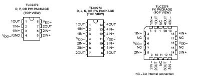
Features: Output Swing Includes Both Supply Rails
Low Noise . . . 9 nV/HZ Typ at f = 1 kHz
Low Input Bias Current . . . 1 pA Typ
Fully Specified for Both Single-Supply and Split-Supply Operation
Common-Mode Input Voltage Range Includes Negative Rail
High-Gain Bandwidth . . . 2.2 MHz Typ
High Slew Rate . . . 3.6 V/s Typ
Low Input Offset Voltage
950 V Max at TA = 25°C
Macromodel Included
Performance Upgrades for the TS272, TS274, TLC272, and TLC274
Available in Q-Temp Automotive HighRel Automotive Applications Configuration Control / Print Support Qualification to Automotive StandardsPinout SpecificationsSupply voltage, VDD+ (see Note 1) . . . . . . . . . . . . . . . . . . . . . . . . . . . . . . . . . . . . . . .. . . . 8 V
Supply voltage, VDD (see Note 1) . . . . . . . . . . . . . . . . . . . . . . . . . . . . . . . . . . . . . . . . . 8 V
Differential input voltage, VID (see Note 2) . . . . . . . . . . . . . . . . . . . . . . . . . . . . . . . . . . . ±16 V
Input voltage, VI (any input, see Note 1) . . . . . . . . . . . . . . . . . . . . . . . . . . . . . . . . . . . . . VDD 0.3 V to VDD+
Input current, II (any input) . . . . . . . . . . . . . . . . . . . . . . . . . . . . . . . . . . . . . . . . . . . . . . . ±5 mA
Output current, IO . . . . . . . . . . . . . . . . . . . . . . . . . . . . . . . . . . . . . . . . . . . . . . . . . . . . . . . ±50 mA
Total current into VDD+ . . . . . . . . . . . . . . . . . . . . . . . . . . . . . . . . . . . . . . . . . . . . . . . . . . . ±50 mA
Total current out of VDD . . . . . . . . . . . . . . . . . . . . . . . . . . . . . . . . . . . . . . . . . . . . . . . .. . ±50 mA
Duration of short-circuit current at (or below) 25°C (see Note 3) . . . . . . . . . . . . . . . . . . . unlimited
Continuous total dissipation . . . . . . . . . . . . . . . . . . . . . . . . . . . . . . . . . . . . . . . . . . . See Dissipation Rating Table
Operating free-air temperature range, TA: C suffix . . . . . . . . . . . . . . . . . . . . . . . . . . . . .. 0°C to 70°C
I suffix . . . . . . . . . . . . . . . . . . . . . . . . . . .. 40°C to 85°C
Q suffix . . . . . . . . . . . . . . . . . . . . . . . . . . . 40°C to 125°C
M suffix . . . . . . . . . . . . . . . . . . . . . . . . . . . 55°C to 125°C
Storage temperature range . . . . . . . . . . . . . . . . . . . . . . . . . . . . . . . . . . . . . . . . . . . . . 65°C to 150°C
Lead temperature 1,6 mm (1/16 inch) from case for 10 seconds: D, N, P or PW package . . . . . . . . 260°C
Lead temperature 1,6 mm (1/16 inch) from case for 60 seconds: J package . . . . . . . . . . . . . . . . . . 300°C
NOTES: 1. All voltage values, except differential voltages, are with respect to the midpoint between VDD+ and VDD .
2. Differential voltages are at IN+ with respect to IN . Excessive current will flow if input is brought below VDD 0.3 V.
3. The output may be shorted to either supply. Temperature and/or supply voltages must be limited to ensure that the maximum dissipation rating is not exceeded.DescriptionThe TLC2272 and TLC2274 are dual and quadruple operational amplifiers from Texas Instruments. Both devices exhibit rail-to-rail output performance for increased dynamic range in single- or split-supply applications. The TLC227x family offers 2 MHz of bandwidth and 3 V/ms of slew rate for higher speed applications. These devices offer comparable ac performance while having better noise, input offset voltage, and power dissipation than existing CMOS
operational amplifiers. The TLC227x has a noise voltage of 9 nV//Hz, two times lower than competitive solutions.
The TLC227x, exhibiting high input impedance and low noise, is excellent for small-signal conditioning for high-impedance sources, such as piezoelectric transducers. Because of the micropower dissipation levels, these devices work well in hand-held monitoring and remote-sensing applications. In addition, the rail-to-rail output feature, with single- or split-supplies, makes this family a great choice when interfacing with analog-to-digital converters (ADCs). For precision applications, the TLC227xA family is available and has a maximum input offset voltage of 950 V. This family is fully characterized at 5 V and ±5 V.
The TLC2272/4 also makes great upgrades to the TLC272/4 or TS272/4 in standard designs. They offer increased output dynamic range, lower noise voltage, and lower input offset voltage. This enhanced feature set allows them to be used in a wider range of applications. For applications that require higher output drive and wider input voltage range, see the TLV2432 and TLV2442 devices.
If the design requires single amplifiers, please see the TLV2211/21/31 family. These devices are single rail-to-rail operational amplifiers in the SOT-23 package. Their small size and low power consumption, make them ideal for high density, battery-powered equipment.

 TLC227xA Data Sheet


