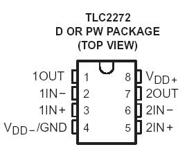
Pinout Specifications
Supply voltage, VDD+ (see Note 1) . . . . . . . . . . . . . . . . . . . . . . . . . . . . . . . . . . . . . . . . . . . . . . . . .8 V
Supply voltage, VDD− (see Note 1) . . . . . . . . . . . . . . . . . . . . . . . . . . . . . . . . . . . . . . . . . . . . . . . −8 V
Differential input voltage, VID (see Note 2) . . . . . . . . . . . . . . . . . . . . . . . . . . . . . . . . . . . . . . . . ±16 V
Input voltage range, VI (any input, see Note 1) . . . . . . . . . . . . . . . . . . . . . . . . . VDD− − 0.3 V to VDD+
Input current, II (any input) . . . . . . . . . . . . . . . . . . . . . . . . . . . . . . . . . . . . . . . . . . . . . . . . . . . . ±5 mA
Output current, IO . . . . . . . . . . . . . . . . . . . . . . . . . . . . . . . . . . . . . . . . . . . . . . . . . . . . . . . . . . .±50 mA
Total current into VDD+ . . . . . . . . . . . . . . . . . . . . . . . . . . . . . . . . . . . . . . . . . . . . . . . . . . . . . . .±50 mA
Total current out of VDD− . . . . . . . . . . . . . . . . . . . . . . . . . . . . . . . . . . . . . . . . . . . . . . . . . . . . ..±50 mA
Duration of short-circuit current at (or below) 25°C (see Note 3) . . . . . . . . . . . . . . . . . . . . . .unlimited
Continuous total dissipation . . . . . . . . . . . . . . . . . . . . . . . . . . . . . . . . . . . See Dissipation Rating Table
Operating free-air temperature range, TA . . . . . . . . . . . . . . . . . . . . . . . . . . . . . . . . . −55°C to 125°C
Storage temperature range (see Note 4) . . . . . . . . . . . . . . . . . . . . . . . . . . . . . . . . . −65°C to 150°C
Lead temperature 1,6 mm (1/16 inch) from case for 10 seconds: D or PW package . . . . . . . . . .260°C
† Stresses beyond those listed under "absolute maximum ratings" may cause permanent damage to the device. These are stress ratings only, and functional operation of the device at these or any other conditions beyond those indicated under "recommended operating conditions" is not implied. Exposure to absolute-maximum-rated conditions for extended periods may affect device reliability.
NOTES: 1. All voltage values, except differential voltages, are with respect to the midpoint between VDD+ and VDD −.
2. Differential voltages are at IN+ with respect to IN −. Excessive current will flow if input is brought below VDD− − 0.3 V.
3. The output may be shorted to either supply. Temperature and/or supply voltages must be limited to ensure that the maximum dissipation rating is not exceeded.
4. Long term high-temperature storage and/or extended use at maximum recommended operating conditions may result in a reduction of overall device life. See http://www.ti.com/ep_quality for additional information on enhanced plastic packaging.
DescriptionThe TLC2272A and TLC2274A are dual and quadruple operational amplifiers from Texas Instruments. Both devices exhibit rail-to-rail output performance for increased dynamic range in single- or split-supply applications. The TLC227xA family offers 2 MHz of bandwidth and 3 V/µs of slew rate for higher speed applications. These devices offer comparable ac performance while having better noise, input offset voltage, and power dissipation than existing CMOS operational amplifiers. The TLC227xA has a noise voltage of 9 nV/Hz, two times lower than competitive solutions.
The TLC227xA, exhibiting high input impedance and low noise, is excellent for small-signal conditioning for high-impedance sources, such as piezoelectric transducers. Because of the micropower dissipation levels, these devices work well in hand-held monitoring and remote-sensing applications. In addition, the rail-to-rail output feature, with single- or split-supplies, makes this family a great choice when interfacing with analog-to-digital converters (ADCs). For precision applications, the LC227xA family has a maximum input offset voltage of 950 µV. This family is fully characterized at 5 V and ±5 V.

 TLC2272A Data Sheet


