TLC1550I

Features: ·Power Dissipation . . . 40 mW Max·Advanced LinEPICETM Single-Poly Process·Provides Close Capacitor Matching for·Better Accuracy·Fast Parallel Processing for DSP and mP Interface·Either External or Internal Clock Can Be Used·Conversion Time . . . 6 ms·Total Unadjusted Error . . . ±1 LSB ...

product image

TLC1550I Picture
SeekIC No. : 004520430 Detail

TLC1550I: Features: ·Power Dissipation . . . 40 mW Max·Advanced LinEPICETM Single-Poly Process·Provides Close Capacitor Matching for·Better Accuracy·Fast Parallel Processing for DSP and mP Interface·Either Ex...

floor Price/Ceiling Price

Part Number:
TLC1550I
Supply Ability:
5000

Price Break

  • Qty
  • 1~5000
  • Unit Price
  • Negotiable
  • Processing time
  • 15 Days
Total Cost: $ 0.00

SeekIC Buyer Protection PLUS - newly updated for 2013!

  • Escrow Protection.
  • Guaranteed refunds.
  • Secure payments.
  • Learn more >>

Month Sales

268 Transactions

Rating

evaluate  (4.8 stars)

Upload time: 2025/1/11

Payment Methods

All payment methods are secure and covered by SeekIC Buyer Protection PLUS.

Notice: When you place an order, your payment is made to SeekIC and not to your seller. SeekIC only pays the seller after confirming you have received your order. We will also never share your payment details with your seller.
Product Details

Description


Features:

·Power Dissipation . . . 40 mW Max
·Advanced LinEPICETM Single-Poly Process
·Provides Close Capacitor Matching for
·Better Accuracy
·Fast Parallel Processing for DSP and mP Interface
·Either External or Internal Clock Can Be Used
·Conversion Time . . . 6 ms
·Total Unadjusted Error . . . ±1 LSB Max
·CMOS Technology


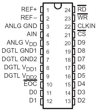
Pinout

  Connection Diagram


Specifications

Supply voltage, VDD1, VDD2, and VDD3 (see Note 1) . . . . . . . . . . . . . . . . . . . . . . . . . . . . . . . . .6.5 V
Input voltage range, VI (any input) . . . . . . . . . . . . . . . . . . . . . . . . . . . . . . . . 0.3 V to VDD + 0.3 V
Output voltage range, VO . . . . . . . . . . . . . . . . . . . . . . . . . . . . . . . . . . . . . . . .0.3 V to VDD + 0.3 V
Peak input current (any digital input) . . . . . . . . . . . . . . . . . . . . . . . . . . . . . . . . . . . . . . . . . . ±10 mA
Peak total input current (all inputs) . . . . . . . . . . . . . . . . . . . . . . . . . . . . . . . . . . . . . . . . . . . .±30 mA
Operating free-air temperature range, TA: TLC1550I, TLC1551I . . . . . . . . . . . . . . .40°C to 85°C
Operating free-air temperature range, TA: TLC1550M . . . . . . . . . . . . . . . . . . . . . .55°C to 125°C
Storage temperature range, Tstg . . . . . . . . . . . . . . . . . . . . . . . . . . . . . . . . . . . . . .65°C to 150°C
Case temperature for 10 seconds: FK or FN package . . . . . . . . . . . . . . . . . . . . . . . . . . . . . . . 260°C
Lead temperature 1,6 mm (1/16 inch) from the case for 10 seconds: J or NW package . . . . . .260°C


Description

The TLC1550x and TLC1551 are data acquisition analog-to-digital converters (ADCs) using a 10-bit, switched-capacitor, successive-approximation network. A high-speed, 3-state parallel port directly interfaces to a digital signal processor (DSP) or microprocessor (mP) system data bus. D0 through D9 are the digital output terminals with D0 being the least significant bit (LSB). Separate power terminals for the analog and digital portions minimize noise pickup in the supply leads. Additionally, the digital power is divided into two parts to separate the lower current logic from the higher current bus drivers. An external clock can be applied to CLKIN to override the internal system Dlock if desired.

The TLC1550I and TLC1551I are characterized for operation from 40°C to 85°C. The TLC1550M is characterized over the full military range of 55°C to 125°C.


Customers Who Bought This Item Also Bought

Margin,quality,low-cost products with low minimum orders. Secure your online payments with SeekIC Buyer Protection.
Undefined Category
Circuit Protection
Potentiometers, Variable Resistors
Batteries, Chargers, Holders
Resistors
Audio Products
View more