TLC1078

Features: ` Power Dissipation as Low as 10 mW Typ Per Amplifier` Operates on a Single Silver-Oxide Watch Battery, VDD = 1.4 V Min` VIO . . . 450 V/850 mV Max in DIP and Small-Outline Package (TLC1078/79)` Input Offset Voltage Drift . . . 0.1 mV/Month Typ, Including the First 30 Days` High-impedanc...

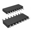
product image

TLC1078 Picture
SeekIC No. : 004520406 Detail

TLC1078: Features: ` Power Dissipation as Low as 10 mW Typ Per Amplifier` Operates on a Single Silver-Oxide Watch Battery, VDD = 1.4 V Min` VIO . . . 450 V/850 mV Max in DIP and Small-Outline Package (TLC107...

floor Price/Ceiling Price

Part Number:
TLC1078
Supply Ability:
5000

Price Break

  • Qty
  • 1~5000
  • Unit Price
  • Negotiable
  • Processing time
  • 15 Days
Total Cost: $ 0.00

SeekIC Buyer Protection PLUS - newly updated for 2013!

  • Escrow Protection.
  • Guaranteed refunds.
  • Secure payments.
  • Learn more >>

Month Sales

268 Transactions

Rating

evaluate  (4.8 stars)

Upload time: 2024/12/27

Payment Methods

All payment methods are secure and covered by SeekIC Buyer Protection PLUS.

Notice: When you place an order, your payment is made to SeekIC and not to your seller. SeekIC only pays the seller after confirming you have received your order. We will also never share your payment details with your seller.
Product Details

Description


Features:

` Power Dissipation as Low as 10 mW Typ Per Amplifier
` Operates on a Single Silver-Oxide Watch Battery, VDD = 1.4 V Min
` VIO . . . 450 V/850 mV Max in DIP and Small-Outline Package (TLC1078/79)
` Input Offset Voltage Drift . . . 0.1 mV/Month Typ, Including the First 30 Days
` High-impedance LinCMOSE Inputs IIB = 0.6 pA Typ
` High Open-Loop Gain . . . 800000 Typ
` Output Drive Capability > 20 mA
` Slew Rate . . . 47 V/ms Typ
` Common-Mode Input Voltage Range Extends Below the Negative Rail
` Output Voltage Range Includes Negative Rail
` On-Chip ESD-Protection Circuitry
` Small-Outline Package Option Also Available in Tape and Reel


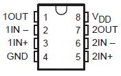
Pinout

  Connection Diagram


Specifications

Supply voltage, VDD (see Note 1) . . . . . . . . . .  . .. . . . . . . . . . . . . . . . . 18 V
Differential input voltage, VID (see Note 2) . . . . . .  . . . . . . . . . . . . . . ±VDD
Input voltage range, VI (any input) . . . . . . . . . . . .  . . . . . . . 0.3 V to VDD
Input current, II (each input) . . . . . . . . . . . . . . . . . . . . . . . . . . . . . . ± 5 mA
Output current, IO (each output) . . . . . . . . . . . . . . . . . . . . . . . . . . ± 30 mA
Total current into VDD (see Note 3) . . . . . . . . . . . . . . . . . . . . . . . . . . 45 mA
Duration of short-circuit at (or below)
                                           TA = 25 (see Note 3) . . . . . . . . . . . . unlimited
Continuous total power dissipation . . . . . . .. . see Dissipation Rating Table
Operating free-air temperature range, TA: C suffix . .. . . . . . . . . 0 to 70
                                                                   I suffix  . . . . . . . . 40 to 85
                                                                   M suffix   . . . . . . 55 to 125
Storage temperature range . . . . . . .  . . . . . . . . . . . . . . . . . 65 to 150
Case temperature for 60 seconds: FK package         . . . . . . . . . . . . . 260
Lead temperature 1,6 mm (1/16 inch)
from case for 10 seconds: D or P package         . . . . . . . . . . . . . . . . . 260
Lead temperature 1,6 mm (1/16 inch) from
        case for 60 seconds: JG package         . . . . . . . . . . . . . . . . . . . . 300
† Stresses beyond those listed under "absolute maximum ratings" may cause permanent damage to the device. These are stress ratings only, and functional operation of the device at these or any other conditions beyond those indicated under "recommended operating conditions" is not implied. Exposure to absolute-maximum-rated conditions for extended periods may affect device reliability.
NOTES: 1. All voltage values, except differential voltages, are with respect to network ground.
2. Differential voltages are at IN+ with respect to IN .
3. The output may be shorted to either supply. Temperature and/or supply voltages must be limited to ensure that the maximum dissipation ratings are not exceeded.


Description

The TLC107x operational amplifiers offer ultralow offset voltage, high gain, 110-kHz bandwidth,47-V/ms slew rate, and just 150-mW power dissipation per amplifier.

With a supply voltage of 1.4 V, common-mode input to the negative rail, and output swing to the negative rail, the TLC107xC is an ideal solution for low-voltage battery-operated systems. The 20-mA output drive capability means that the TLC107x can easily drive small resistive and large capacitive loads when needed, while maintaining ultra-low standby power dissipation.

Since this device is functionally compatible as well as pin compatible with the TLC27L2/4 and TLC27L7/9, the TLC107x easily upgrades existing designs that can benefit from its improved performance.


Customers Who Bought This Item Also Bought

Margin,quality,low-cost products with low minimum orders. Secure your online payments with SeekIC Buyer Protection.
Batteries, Chargers, Holders
Crystals and Oscillators
Industrial Controls, Meters
Discrete Semiconductor Products
Prototyping Products
DE1
View more