TLC1225M

Features: • Advanced LinCMOSE Technology• Self Calibration Eliminates Expensive Trimming at Factory and Offset Adjustment in the Field• 12-Bit-Plus-Sign Resolution• 12-Bit Linearity• 12-ms Conversion Period at fclock = 2 MHz†• Compatible With All Microproc...

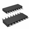
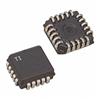
product image

TLC1225M Picture
SeekIC No. : 004520413 Detail

TLC1225M: Features: • Advanced LinCMOSE Technology• Self Calibration Eliminates Expensive Trimming at Factory and Offset Adjustment in the Field• 12-Bit-Plus-Sign Resolution• 12-Bit Li...

floor Price/Ceiling Price

Part Number:
TLC1225M
Supply Ability:
5000

Price Break

  • Qty
  • 1~5000
  • Unit Price
  • Negotiable
  • Processing time
  • 15 Days
Total Cost: $ 0.00

SeekIC Buyer Protection PLUS - newly updated for 2013!

  • Escrow Protection.
  • Guaranteed refunds.
  • Secure payments.
  • Learn more >>

Month Sales

268 Transactions

Rating

evaluate  (4.8 stars)

Upload time: 2025/1/11

Payment Methods

All payment methods are secure and covered by SeekIC Buyer Protection PLUS.

Notice: When you place an order, your payment is made to SeekIC and not to your seller. SeekIC only pays the seller after confirming you have received your order. We will also never share your payment details with your seller.
Product Details

Description


Features:

• Advanced LinCMOSE Technology
• Self Calibration Eliminates Expensive
  Trimming at Factory and Offset Adjustment
  in the Field
• 12-Bit-Plus-Sign Resolution
• 12-Bit Linearity
• 12-ms Conversion Period at fclock = 2 MHz†
• Compatible With All Microprocessors
• Single 5-V and ±5-V Supply Operation
• True Differential Analog Voltage Inputs
  With Vref to Vref Differential Input Range
• For Single 5-V Supply, Input
  Common-Mode Voltage Range is 0 V to 5 V
• For ±5-V Supplies, Input Common-Mode
  Voltage Range is 5 V to 5 V
• Unipolar or Bipolar Operation
• 2s-Complement Output
• Low Power
  85 mW Max on TLC1225I
  87.5 mW Max on TLC1225M


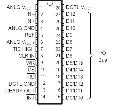
Pinout

  Connection Diagram


Specifications

Supply voltage (ANLG VCC+ and DGTL VCC) (see Note 1) . . . . . . . . . . . . . . . . . . . . . . . . . . . . . . . . 7.5 V
Supply voltage, ANLG VCC . . . . . . . . . . . . . . . . . . . . . . . . . . . . . . . . . . . . . . . . . . . . . . . . . . . . . .7.5 V
Differential supply voltage, ANLG VCC+ ANLG VCC . . . . . . . . . . . . . . . . . . . . . . . . . . . . . . . . . . .   15 V
Clock input voltage range . . . . . . . . . . . . . . . . . . . . . . . . . . . . . . . . . . . . . . . . . . .  0.3 V to VCC + 0.3 V
Control input voltage range . . . . . . . . . . . . . . . . . . . . . . . . . . . . . . . . . . . . . . . . . . 0.3 V to VCC + 0.3 V
Analog input (IN+, IN) voltage range, VI+ and VI . . . . . . . . . ANLG VCC 0.3 V to ANLG VCC+ +0.3 V
Reference voltage range, Vref . . . . . . . . . . . . . . . . . . . . . . . . . . . . . . . . . . . 0.3 V to ANLG VCC+ +0.3 V
Voltage range, TIE HIGH . . . . . . . . . . . . . . . . . . . . . . . . . . . . . . . . . . . . . . .  0.3 V to ANLG VCC+ +0.3 V
Output voltage range . . . . . . . . . . . . . . . . . . . . . . . . . . . . . . . . . . . . . . . . . . . 0.3 V to DGTL VCC +0.3 V
Input current (per pin) . . . . . . . . . . . . . . . . . . . . . . . . . . . . . . . . . . . . . . . . . . . . . . . . . . . . . . . . . . .±5 mA
Input current (per package) . . . . . . . . . . . . . . . . . . . . . . . . . . . . . . . . . . . . . . . . . . . . . . . . . . . . . .±20 mA
Continued total dissipation . . . . . . . . . . . . . . . . . . . . . . . . . . . . . . . . . . . . . . See Dissipation Rating Table
Operating free-air temperature range, TA:TLC1225I . . . . . . . . . . . . . . . . . . . . . . . . . . . . . .40°C to 85°C
TLC1225M . . . . . . . . . . . . . . . . . . . . . . . . . . . . . . . . . . . . . . . . . . . . . . . . . . . . . . . . . . . . . 55°C to 125°C
Storage temperature range . . . . . . . . . . . . . . . . . . . . . . . . . . . . . . . . . . . . . . . . . . . . . . . . 65°C to 150°C
Case temperature for 60 seconds: FK or FN package . . . . . . . . . . . . . . . . . . . . . . . . . . . . . . . . . . . . .260°C
Lead temperature 1,6 mm (1/16 inch) from the case for 10 seconds: NW package . . . . . . . . . . . . .   260°C
Lead temperature 1,6 mm (1/16 inch) from the case for 60 seconds: J package . . . . . . . . . . . . . . . . 300°C
† Stresses beyond those listed under "absolute maximum ratings" may cause permanent damage to the device. These are stress ratings only, and
functional operation of the device at these or any other conditions beyond those indicated under "recommended operating conditions" is not
implied. Exposure to absolute-maximum-rated conditions for extended periods may affect device reliability.
NOTE 1: All analog voltages are referred to ANLG GND, and all digital voltages are referred to DGTL GND.


Description

The TLC1225I and TLC1225M converters are manufactured with Texas Instruments highly efficient Advanced LinCMOSE technology. The TLC1225I and TLC1225M CMOS analog-todigital converters (ADCs) can be operated with a single 5-V supply or with ±5-V supplies. The differential input range is Vref to Vref in both supply configurations. The common-mode input range is ANLG VCC to ANLG VCC+. For single 5-V supply operation, grounding IN corresponds to standard unipolar conversion. For ±5-V supply operation, grounding IN corresponds to standard bipolar conversion. Conversion is performed via the successive-approximation method. The TLC1225x outputs the converted data in a parallel word and interfaces directly to a 16-bit data bus. Negative numbers are given in the 2s-complement data format. All digital signals are fully TTL and CMOS compatible.

This converter TLC1225I and TLC1225M uses a self-calibration technique by which seven of the internal capacitors in the capacitive array of the A/D conversion circuitry can be automatically calibrated. The internal capacitors are calibrated during a nonconversion capacitor-calibrate cycle in which all seven of the internal capacitors are calibrated at the same time. A conversion period requires only 24 clock cycles. Self calibration requires 300 clock cycles. The calibration or conversion cycle can be initiated at any time by issuing the proper command word to the data bus. The self-calibrating technique eliminates the need for expensive trimming of thin-film resistors at the factory and provides excellent performance at low cost.

The TLC1225I is characterized for operation from 40°C to 85°C. The TLC1225M is characterized over the full military temperature range of 55°C to 125°C.


Customers Who Bought This Item Also Bought

Margin,quality,low-cost products with low minimum orders. Secure your online payments with SeekIC Buyer Protection.
Computers, Office - Components, Accessories
Static Control, ESD, Clean Room Products
LED Products
Memory Cards, Modules
Tapes, Adhesives
803
View more