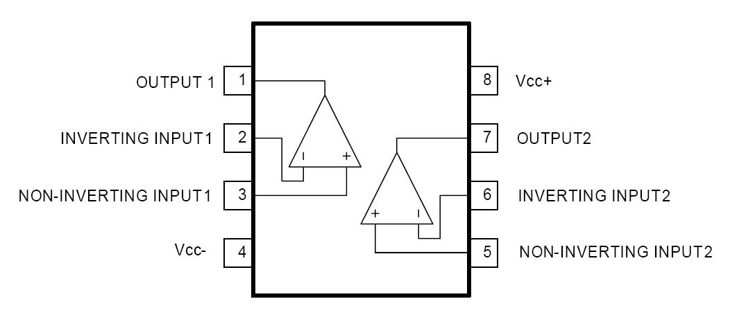
Features: ` Very low power consumption` Wide common-mode (up to VCC+ ) and differential voltage range` Low input bias and offset current` Output short-circuit protection` High input impedance J-FET input stage` Internal frequency compensation` Latch up free operation` Typical supply current: 200AP...
TL062-D08: Features: ` Very low power consumption` Wide common-mode (up to VCC+ ) and differential voltage range` Low input bias and offset current` Output short-circuit protection` High input impedance J-FET ...
SeekIC Buyer Protection PLUS - newly updated for 2013!
268 Transactions
All payment methods are secure and covered by SeekIC Buyer Protection PLUS.
Parameter | SYMBOL | RATINGS | Units |
Supply Voltage (note 1) | VCC | ±18 | V |
Input Voltage (note 2) | VIN | ±15 | V |
Differential Input Voltage (note 3) | VI(DIFF) | ±30 | V |
Power Dissipation | PD | 680 | mW |
Output Short-Circuit Duration (Note 4) | Infinite | ||
Operating Free Air Temperature | TOPR | 0 ~ +70 | °C |
Storage Temperature | TSTG | -65 ~ +150 | °C |
Notes: 1. All voltage values, except differential voltage, are with respect to the zero reference level (ground) of the
supply voltages where the zero reference level is the midpoint between VCC- and VCC+.
2. The magnitude of the input voltage must never exceed the magnitude of the supply voltage or 15 volts,
whichever is less.
3. Differential voltages are at the non-inverting input terminal with respect to the inverting input terminal.
4. The output may be shorted to ground or to either supply. Temperature and/or supply voltages must be
limited to ensure that the dissipation rating is not exceeded.
The UTC TL062 is a high speed J-FET input dual operational amplifier. It incorporates well matched, high voltage J-FET and bipolar transistors in a monolithic integrated circuit. The device features high slew rates, low input bias and offset currents, and low offset voltage temperature coefficient.