THS6053

Features: Remote Terminal ADSL Line Driver Ideal for Both Full Rate ADSL and G.Lite Compatible With 1:1 Transformer Ratio Low 2.7 pA/Hz Noninverting Current Noise Reduces Noise Feedback Through Hybrid Into Downstream Channel Wide Supply Voltage Range ±5 V to ±15 V Ideal for ±12-V Operation Wide Ou...

product image

THS6053 Picture
SeekIC No. : 004518924 Detail

THS6053: Features: Remote Terminal ADSL Line Driver Ideal for Both Full Rate ADSL and G.Lite Compatible With 1:1 Transformer Ratio Low 2.7 pA/Hz Noninverting Current Noise Reduces Noise Feedback Through Hybr...

floor Price/Ceiling Price

Part Number:
THS6053
Supply Ability:
5000

Price Break

  • Qty
  • 1~5000
  • Unit Price
  • Negotiable
  • Processing time
  • 15 Days
Total Cost: $ 0.00

SeekIC Buyer Protection PLUS - newly updated for 2013!

  • Escrow Protection.
  • Guaranteed refunds.
  • Secure payments.
  • Learn more >>

Month Sales

268 Transactions

Rating

evaluate  (4.8 stars)

Upload time: 2025/1/12

Payment Methods

All payment methods are secure and covered by SeekIC Buyer Protection PLUS.

Notice: When you place an order, your payment is made to SeekIC and not to your seller. SeekIC only pays the seller after confirming you have received your order. We will also never share your payment details with your seller.
Product Details

Description


Features:

 Remote Terminal ADSL Line Driver
Ideal for Both Full Rate ADSL and G.Lite
Compatible With 1:1 Transformer Ratio
Low 2.7 pA/Hz Noninverting Current Noise
Reduces Noise Feedback Through Hybrid Into Downstream Channel
Wide Supply Voltage Range ±5 V to ±15 V
Ideal for ±12-V Operation
Wide Output Swing
42 Vpp Differential Output Voltage, RL = 200 , ±12-V Supply
High Output Current
175 mA (typ)
High Speed
110 MHz (3 dB, G=8, ±12 V)
1500 V/s Slew Rate (G = 8, ±12 V)
Low Distortion, Single-Ended, G = 8
83 dBc (250 kHz, 2 Vpp, 100- load)
Low Power Shutdown (THS6053)
300-A Total Standby Current
Thermal Shutdown and Short Circuit Protection
Standard SOIC, SOIC PowerPAD, and TSSOP PowerPAD™Package
Evaluation Module Available


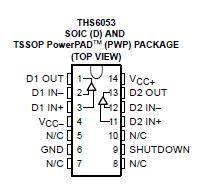
Pinout

  Connection Diagram


Specifications

Supply voltage, VCC+ to VCC . . . . . . . . . . . . . . . . . . . . . . . . . . . . . . . . . . . . . . . . . . . . . . . . . . . . . . . . . 33 V
Input voltage . . . . . . . . . . . . . . . . . . . . . . . . . . . . . . . . . . . . . . . . . . . . . . . . . . . . . . . . . . . . . . . . . . . . . ± VCC
Output current (see Note 1) . . . . . . . . . . . . . . . . . . . . . . . . . . . . . . . . . . . . . . . . . . . . . . . . . . . . . . . . . 275 mA
Differential input voltage . . . . . . . . . . . . . . . . . . . . . . . . . . . . . . . . . . . . . . . . . . . . . . . . . . . . . . . . . . . . . ± 4 V
Maximum junction temperature . . . . . . . . . . . . . . . . . . . . . . . . . . . . . . . . . . . . . . . . . . . . . . . . . . . . . . . 150°C
Total power dissipation at (or below) 25°C free-air temperature . . . . . . . . . . . See Dissipation Ratings Table
Operating free-air temperature, TA: Commercial . . . . . . . . . . . . . . . . . . . . . . . . . . . . . . . . . . . . . 0°C to 70°C
                                                         Industrial . . . . . . . . . . . . . . . . . . . . . . . . . . . . . . . . . . . . 40°C to 85°C
Storage temperature, Tstg : Commercial . . . . . . . . . . . . . . . . . . . . . . . . . . . . . . . . . . . . . . . . 65°C to 125°C
                                             Industrial . . . . . . . . . . . . . . . . . . . . . . . . . . . . . . . . .. . .  . . . . . 65°C to 125°C
Lead temperature 1,6 mm (1/16 inch) from case for 10 seconds . . . . . . . . . . . . . . . . .. . . . . . . . . . . . . . 300°C
† Stresses beyond those listed under "absolute maximum ratings" may cause permanent damage to the device. These are stress ratings only, and functional operation of the device at these or any other conditions beyond those indicated under "recommended operating conditions" is not implied. Exposure to absolute-maximum-rated conditions for extended periods may affect device reliability.
NOTE 1: The THS6052 and THS6053 may incorporate a PowerPAD™on the underside of the chip. This acts as a heatsink and must be connected to a thermally dissipating plane for proper power dissipation. Failure to do so may result in exceeding the maximum junction temperature which could permanently damage the device. See TI technical brief SLMA002 for more information about utilizing the PowerPAD™ thermally enhanced package.


Description

The THS6052/3 is a high-speed line driver ideal for driving signals from the remote terminal to the central office in asymmetrical digital subscriber line (ADSL) applications. It can operate from ±12-V supply voltages while drawing only 5.2 mA of supply current per channel. It offers low 83 dBc total harmonic distortion driving a 100- load (2 Vpp). The THS6052/3 offers a high 42-Vpp differential output swing across a 200- load from a ±12-V supply. The THS6053 features a low-power shutdown mode, consuming only 300 A quiescent current per channel. The THS6052/3 is packaged in a standard SOIC, SOIC PowerPAD™, and TSSOP PowerPAD™packages.


Customers Who Bought This Item Also Bought

Margin,quality,low-cost products with low minimum orders. Secure your online payments with SeekIC Buyer Protection.
Cables, Wires - Management
Optical Inspection Equipment
Power Supplies - External/Internal (Off-Board)
Integrated Circuits (ICs)
Power Supplies - Board Mount
View more