Features: * Remote Terminal ADSL Line Driver
Ideal for Both Full Rate ADSL and G.Lite
Compatible With 1:1 Transformer Ratio
* Low 2.1 pA/Hz Noninverting Current Noise
Reduces Noise Feedback Through Hybrid Into Downstream Channel
* Wide Supply Voltage Range ±5 V to ±15 V
Ideal for ±12-V Operation
* Wide Output Swing
43-Vpp Differential Output Voltage, RL = 200 Ω, ±12-V Supply
* High Output Current
350 mA (typ)
* High Speed
120 MHz (3 dB, G=1, ±12 V, RL = 25 Ω)
1200 V/µs Slew Rate (G = 4, ±12 V)
* Low Distortion, Single-Ended, G = 4
79 dBc (250 kHz, 2 Vpp, 100-Ω load)
* Low Power Shutdown (THS6043)
300-µA Total Standby Current
* Thermal Shutdown and Short-Circuit=Protection
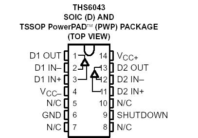
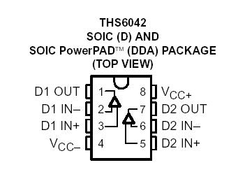
* Standard SOIC, SOIC PowerPAD and TSSOP PowerPAD Package
* Evaluation Module AvailableApplicationdevice protection features
The THS6042/3 have two built-in features that protect the devices against improper operation. The first protection mechanism is output current limiting. Should the output become shorted to ground, the output current is automatically limited to the value given in the data sheet. While this protects the output against excessive current, the device internal power dissipation increases due to the high current and large voltage drop across the output transistors. Continuous output shorts are not recommended and could damage the device.
The second built-in protection feature is thermal shutdown. Should the internal junction temperature rise above approximately 180�C, the device automatically shuts down. Such a condition could exist with improper heat sinking or if the output is shorted to ground. When the abnormal condition is fixed, the internal thermal shutdown circuit automatically turns the device back on.
thermal information PowerPAD
The THS6042/3 are available packaged in thermally-enhanced PowerPAD packages. These packages are constructed using a downset leadframe upon which the die is mounted [see Figure 40(a) and Figure 40(b)]. This arrangement results in the lead frame being exposed as a thermal pad on the underside of the package [see Figure 40(c)]. Because this thermal pad has direct thermal contact with the die, excellent thermal performance can be achieved by providing a good thermal path away from the thermal pad.
The PowerPAD package allows for both assembly and thermal management in one manufacturing operation. During the surface-mount solder operation (when the leads are being soldered), the thermal pad can also be soldered to a copper area underneath the package. Through the use of thermal paths within this copper area,heat can be conducted away from the package into either a ground plane or other heat dissipating device. This is discussed in more detail in the PCB design considerations section of this document.
The PowerPAD package represents a breakthrough in combining the small area and ease of assembly of surface mount with the, heretofore, awkward mechanical methods of heatsinking.
Pinout

SpecificationsSupply voltage, VCC+ to VCC . . . . . . . . . . . . . . . . . . . . . . . . . . . . . . . . . . . . . . . . . . . . . . . . . . . . . . . . . . . ... . . .33 V
Input voltage . . . . . . . . . . . . . . . . . . . . . . . . . . . . . . . . . . . . . . . . . . . . . . . . . . . . . . . . . . . . . . . . . . . . . . . . . . . .± VCC
Output current (see Note 1) . . . . . . . . . . . . . . . . . . . . . . . . . . . . . . . . . . . . . . . . . . . . . . . . . . . . . . . . . . . ...... . .450 mA
Differential input voltage . . . . . . . . . . . . . . . . . . . . . . . . . . . . . . . . . . . . . . . . . . . . . . . . . . . . . . . . . . . . . . . . . . . ± 4 V
Maximum junction temperature . . . . . . . . . . . . . . . . . . . . . . . . . . . . . . . . . . . . . . . . . . . . . . . . . . . . . . . . ... . . .150°C
Total power dissipation at (or below) 25°C free-air temperature See Dissipation Ratings Table . . . . . . . . . . .
Operating free-air temperature, TA: Commercial . . . . . . . . . . . . . . . . . . . . . . . . . . . . . . . . . . . . . . ....... . 0°C to 70°C
Industrial . . . . . . . . . . . . . . . . . . . . . . . . . . . . . . . . . . . . . . . ..............................................................40°C to 85°C
Storage temperature, Tstg : Commercial . . . . . . . . . . . . . . . . . . . . . . . . . . . . . . . . . . . . . . . . . .... . .65°C to 125°C
Industrial . . . . . . . . . . . . . . . . . . . . . . . . . . . . . . . . . . . . . . . . . . . ................................................ . .65°C to 125°C
Lead temperature 1,6 mm (1/16 inch) from case for 10 seconds . . . . . . . . . . . . . . . . . . . . . . . . ........... . . . . . .300°C
NOTE 1: The THS6042 and THS6043 may incorporate a PowerPAD on the underside of the chip. This acts as a heatsink and must be connected to a thermally dissipating plane for proper power dissipation. Failure to do so may result in exceeding the maximum junction temperature which could permanently damage the device. See TI Technical Brief SLMA002 for more information about utilizing the PowerPAD Thermally enhanced package.
DescriptionThe THS6042/3 is a high-speed line driver ideal for driving signals from the remote terminal to the central office in asymmetrical digital subscriber line (ADSL) applications. It can operate from a ±12-V supply voltage while drawing only 8.2 mA of supply current per channel. It offers low 79 dBc total harmonic distortion driving a 100-Ω load (2 Vpp). The THS6042/3 offers a high 43-Vpp differential output swing across a 200-Ω load from a ±12-V supply. The THS6043 features a low-power shutdown mode, consuming only 300 µA quiescent current per channel. The THS6042/3 is packaged in standard SOIC, SOIC PowerPAD, and TSSOP PowerPAD packages.

 THS6042 Data Sheet


