TDA3681

Features: General ` Extremely low noise behaviour and good stability with very small output capacitors ` Second supply pin for regulators 3 and 4 to reduce power dissipation (e.g. via a DC-to-DC converter) ` Three VP-state controlled regulators (regulators 1, 3 and 4) and a power switch ` Regulato...

product image

TDA3681 Picture
SeekIC No. : 004516298 Detail

TDA3681: Features: General ` Extremely low noise behaviour and good stability with very small output capacitors ` Second supply pin for regulators 3 and 4 to reduce power dissipation (e.g. via a DC-to-DC con...

floor Price/Ceiling Price

Part Number:
TDA3681
Supply Ability:
5000

Price Break

  • Qty
  • 1~5000
  • Unit Price
  • Negotiable
  • Processing time
  • 15 Days
Total Cost: $ 0.00

SeekIC Buyer Protection PLUS - newly updated for 2013!

  • Escrow Protection.
  • Guaranteed refunds.
  • Secure payments.
  • Learn more >>

Month Sales

268 Transactions

Rating

evaluate  (4.8 stars)

Upload time: 2025/1/12

Payment Methods

All payment methods are secure and covered by SeekIC Buyer Protection PLUS.

Notice: When you place an order, your payment is made to SeekIC and not to your seller. SeekIC only pays the seller after confirming you have received your order. We will also never share your payment details with your seller.
Product Details

Description


Features:

General
     ` Extremely low noise behaviour and good stability with very small output capacitors
     ` Second supply pin for regulators 3 and 4 to reduce power dissipation (e.g. via a DC-to-DC converter)
     ` Three VP-state controlled regulators (regulators 1, 3 and 4) and a power switch
     ` Regulator 2, reset and ignition buffer operational during load dump and thermal shutdown
     ` Combined control pin for switching regulators 1 and 3
     ` Separate control pins for switching regulator 4 and the power switch
     ` Supply voltage range from -18 to +50 V
     ` Low quiescent current in standby mode (when regulators 1, 3 and 4 and power switch are switched off and ignition input is low)
     ` Hold output for low VP (regulators 1, 3 and 4 and power switch off)
     ` Hold output when one of regulators 1 and 3 and/or 4 is out of regulation
     ` Hold output for foldback mode of power switch and regulators 1, 3 and 4
     ` Hold output for load dump and temperature protection
     ` Reset (push-pull output stage) for regulator 2 and hold output (open-collector output)
     ` Adjustable reset delay time
     ` High supply voltage ripple rejection
     ` Backup capacitor for regulator 2
     ` One independent ignition buffer (active HIGH).
Protections
     ` Reverse polarity safe (down to -18 V without high reverse current)
     ` Able to withstand voltages up to 18 V at the outputs (supply line may be short-circuited)
     ` ESD protection on all pins
     ` Thermal protections
     ` Load dump protection
     ` Foldback current limit protection for regulators 1, 2, 3 and 4
     ` Delayed second current limit protection for the power switch (at short-circuit)
     ` The regulator outputs and the power switch are DC short-circuit safe to ground and supply (VP).


Pinout

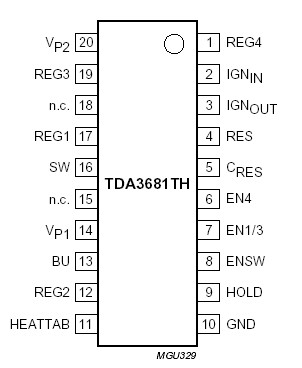
  Connection Diagram


Specifications

SYMBOL PARAMETER CONDITIONS MIN. MAX. UNIT
VP1 supply voltage 1
operating
reverse polarity
jump start
load dump protection
non-operating
t 10 minutes
t 50 ms; tr 2.5 ms
-
-
-
-
18
18
30
50
V
V
V
V
VP2 supply voltage 2
operating
reverse polarity
jump start
load dump protection
non-operating
t 10 minutes
t 50 ms; tr 2.5 ms
-
-
-
-
18
18
30
50
V
V
V
V
Ptot total power dissipation   - 62 W
Tstg storage temperature non-operating -55 +150
Tamb ambient temperature operating -40 +85
Tj junction temperature operating -40 +150


Description

The TDA3681 is a multiple output voltage regulator with a power switch and an ignition buffer. It is intended for use in car radios with or without a microcontroller. The TDA3681 contains the following:

· Four fixed voltage regulators with a foldback current protection (regulators 1, 2, 3 and 4). Regulator 2, which is intended to supply a TDA3681, also operates during load dump and thermal shutdown

· Regulators 3 and 4 have a second supply pin that can be connected to a lower supply voltage (>6.5 V) to reduce the power dissipation

· A power switch with protection, operated by a control input

· Reset and hold outputs that can be used to interface with the microcontroller; the reset signal can be used to call up the TDA3681
· Both supply pins can withstand load dump pulses and negative supply voltages

· Regulator 2, which is in regulation at a backup voltage above 6.5 V

· A provision for the use of a reserve supply capacitor that will hold enough energy for regulator 2 (5 V continuous) to allow a TDA3681 to prepare for loss of voltage

· An ignition input Schmitt trigger with push-pull output stage.


Customers Who Bought This Item Also Bought

Margin,quality,low-cost products with low minimum orders. Secure your online payments with SeekIC Buyer Protection.
Undefined Category
Sensors, Transducers
Power Supplies - Board Mount
Prototyping Products
DE1
View more