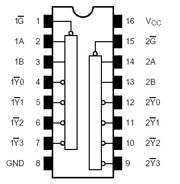
Features: • High speed: tpd = 5.0 ns (typ.) (VCC = 5 V)• Low power dissipation: ICC = 4 µA (max) (Ta = 25°C)• Compatible with TTL outputs: VIL = 0.8 V (max) VIH = 2.0 V (min)• Power down protection is provided on all inputs and outputs.• Balanced propagation del...
TC7MET139AFK: Features: • High speed: tpd = 5.0 ns (typ.) (VCC = 5 V)• Low power dissipation: ICC = 4 µA (max) (Ta = 25°C)• Compatible with TTL outputs: VIL = 0.8 V (max) VIH = 2.0 V (min)...
SeekIC Buyer Protection PLUS - newly updated for 2013!
268 Transactions
All payment methods are secure and covered by SeekIC Buyer Protection PLUS.
Features: Low voltage operation: VCC = 1.8~3.6 VHigh speed operation: tpd = 3.5 ns (max) (VCC = 3....
Features: • Low voltage operation: VCC = 1.8~3.6 V• High speed operation: tpd = 3.0 ns...
Features: • 26 series resistors on outputs.• Low voltage operation: VCC = 1.8~3.6 V...
Characteristics |
Symbol |
Rating |
Unit |
Supply voltage range |
VCC |
−0.5~7.0 |
V |
DC input voltage |
VIN |
−0.5~7.0 |
V |
DC output voltage |
VOUT |
−0.5~7.0 (Note1) −0.5~VCC + 0.5 (Note2) |
V |
Input diode current |
IIK |
−20 |
mA |
Output diode current |
IOK |
±20 (Note3) |
mA |
DC output current |
IOUT |
±25 |
mA |
DC VCC/ground current |
ICC |
±50 |
mA |
Power dissipation |
PD |
180 |
mW |
Storage temperature |
Tstg |
−65~150 |
°C |
The TC7MET139AFK is an advanced high speed CMOS 2 to 4 line decoder/demultiplexer fabricated with silicon gate C2MOS technology.
TC7MET139AFK achieves the high speed operation similar to equivalent bipolar schottky TTL while maintaining the CMOS low power dissipation.
The active low enable input can be used for gating or TC7MET139AFK can be used as a data input for demultiplexing applications.
When the enable input is held High, all four outputs of TC7MET139AFK are fixed at a high logic level independent of the other inputs.
The input voltage of TC7MET139AFK are compatible with TTL output voltage.
The TC7MET139AFK may be used as a level converter for interfacing 3.3 V to This device may be used as a level converter for interfacing 3.3 V to 5 V system.
Input protection and output circuit ensure that 0 to 5.5 V can be applied to the input and output (*) pins without regard to the supply voltage. These structure prevents device destruction due to mismatched supply and input/output voltages such as battery back up, hot board insertion, etc.
*: VCC = 0 V